
Ball grid array (BGA): The process of replacing all the solder balls on a chip’s ball grid array is called BGA rebound. BGA packages have become very popular in the printed circuit board (PCB) design and manufacturing industry. These packages help reduce the size of a PCB and improve its functionality. BGA can withstand the pressure of decreasing product size, and they rarely require maintenance and repair. How are BGA packages repaired, and what steps are BGA reworked? This article mainly describes the “BGA” IC desoldering and BGA reballing process, and the matters needing attention in the repair process.
I. The Matters Need Attention in BGA Chip Repair Process
- Operators must wear electrostatic bracelets.
- Should adjust the airflow and pressure of the hot air gun in advance before desoldering BGA
- The temperature of the hot air gun should be well set in advance (generally controlled at 280~320℃) to prevent the chip from being damaged by excessively high temperature in the process of desoldering. It should not adjust the temperature again during desoldering.
- When desoldering BGA, gently touch the BGA with tweezers to confirm whether the solder on the pad melts away to prevent the BGA pad on the circuit board from being damaged.
- To avoid secondary ball soldering, the orientation marked on the PCBA , should be paid attention to when repairing the BGA.
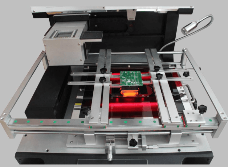
II.Basic equipment and tools to be used in BGA repair
- Intelligent hot air gun. (for BGA desoldering)
- Anti-static maintenance platform and electrostatic bracelet. (need an electrostatic environment)
- Anti-static cleaning device. (for BGA cleaning)
- BGA repair platform. (for BGA soldering)
- High temperature box (used for baking PCBA board)
- Auxiliary equipment: vacuum suction pen, magnifying glass (microscope)
III.Preparation of PCB board baking and related requirements before repair
(1) According to the different exposure times, the PCBA board is given different baking requirements.
(2) Baking time, baking according to the following provisions:
Exposure time ≤2 months, more than 2 months
Baking time 10 hours, 20 hours
Baking temperature 105±5℃, 105±5℃
(3) In front of the baking board, remove the temperature-sensitive components after baking, such as optical fiber, plastic, etc.; Otherwise, it will damage these components due to the high temperature.
(4) For all boards, must complete BGA repair within 10 hours after taking out the boards after baking.
(5) The PCBA board that cannot complete BGA repair work within 10 hours must be placed in a drying oven for preservation. Otherwise, it is easy to lead to sticky back, and damp PCBA is easy to cause PCBA drum when soldering.
VI. Operation steps of BGA chip desoldering and rebelling
Preparation before BGA desoldering
The parameter state of the hot air gun is set as follows: the temperature is 280℃~320℃; desoldering time: 35-55 seconds; Airflow parameters: 6 levels; Finally, the PCBA is placed on the anti-static maintenance platform and fixed.
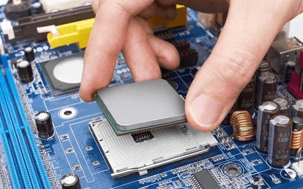
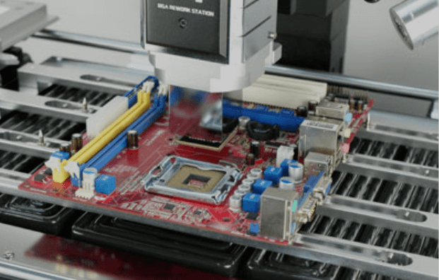
BGA desoldering
Bear in mind that the orientation and position of the chip before desoldering, such as no silkscreen on PCBA, with a marker pen along with all round draw, or next to inject small flux at the bottom of the BGA, choose the suitable size of BGA, BGA soldering nozzle is installed on the hot air gun, will handle the vertical alignment BGA, but pay attention to the nozzle must leave components ca. 4 mm, start the heat gun, The hot air gun will automatically desolder according to the preset parameters. After the end of the desolder, remove the BGA components with a suction pen 2 seconds later. After dismantling the devices, check whether the solder pads of the dismantled machines fall off and whether the traces are scratched, peeled off, or damaged, etc. If will provide abnormal feedback and treatment in time.
BGA and PCB Cleaning
(1) place the board on the work table and use soldering iron absorb redundant residues from the pad, flat pad, cleaning up when placed tin absorption line in solder pad, one hand to lift the suction tin line, put iron absorption tin line, hand gently press iron, residual soldering PCBA or on BGA solder melt and adsorption to absorb tin line, tin absorption line to be moved to the other place, To absorb the rest of the solder, note: do not force on the solder pad to drag, to avoid damage to the solder pad.
(2) After cleaning the pads, use the washing water to clean the PCBA pads. If the virtual soldering CPU needs to replant the ball, use the ultrasonic cleaner (with an anti-static device) to load the washing water, and the removed BGA shall be cleaned and replant the ball for soldering.
Note: For the solder pad cleaning of lead-free devices, the temperature of the soldering iron is required to be < measured value >340+/-40℃; For the cleaning of CBGA and CCGA pads, the temperature of the soldering iron is required to be < measured value >370+/-30℃; there are specific differences in each soldering iron (such as low soldering temperature), please put forward, and the person in charge will make adjustments according to the actual situation. If no adjustment is made, must strictly implement the above requirements.
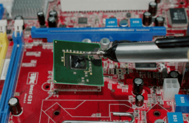
BGA chip reballing
The tin planting of the BGA chip shall be made of laser-punched stencil with single-side horn mesh. The stencil thickness shall be 2mm thick, and the hole wall shall be smooth and tidy. The bottom of the horn hole (the face that contacts the BGA) shall be 10μm~15μm larger than the top (scraping the tin into the spot). Using the tin planting function in the BGA maintenance table above — fixture and stencil, first find the corresponding concave position in the positioning fixture, fix the BGA in the positioning fixture, put the stencil with precise positioning square and round holes on the positioning fixture, and then press the stencil on the fixture with its accessory magnetic press block. The tool has three precision positioning devices (BGA→ fixture → stencil), which can easily and accurately align the stencil mesh with the small solder pad of BGA component.
A small scraper will be a small amount of thick tin slurry scraped to the stencil mesh. When all the mesh has been full, from one end of the stencil will be slowly lifted, BGA chip, a small tin pile, again with a hot air gun to heat it, the BGA tin pile into a uniform array of the tin ball can be. If there is no tin ball in individual pads, a stencil can be pressed again for local tin filling. It cannot be heated together with the stencil because it affects reballing and will be the precise stencil thermal deformation and damage.
BGA chip soldering
Dip a small amount of dense flux on the BGA tin balls and PCBA pads, retrieve the original mark and place the BGA. The BGA should be glued and positioned to prevent it from being blown away by hot wind. However, it should be noted that too much flux should not be put in. Otherwise, excessive bubbles of rosin will cause the chip to shift when heating. PCBA board also is fixed on the BGA rework platform and must be placed level, change the suitable nozzle, nozzle on the BGA chip and left 4 mm, choose BGA to rework stations primary set temperature curve, click on the screen of automatic soldering (note: will not apply pressure on BGA soldering process, easy to cause a short circuit between tin ball under the.)
With the melting of the BGA tin ball and the formation of the PCBA solder pad soldering, and through the surface tension of the tin ball, the chip will automatically center even if there is a deviation from the motherboard. When the BGA repair table is heated, the BGA soldering operation will be completed at this time. However, it should be noted that the BGA repair table will make an alarm sound after heating. At this time, do not move the BGA repair table and PCBA board because the BGA repair table and PCBA board are in a high temperature and unsolidified state. It must wait for 40 seconds before the BGA repair table, and PCBA cools down.
Inspection of BGA soldering and cleaning of PCBA board
1. After the completion of soldering, BGA components and PCBA should be cleaned by washing plate water to remove excess flux and possible tin scraps.2. with the help of a magnifying glass lamp has been soldered on PCBA, BGA component to check whether mainly chips on the point of view, the parallel with PCBA, whether the corresponding has not appeared around the solder overflow, short circuit, etc., even if appeared above any kind of need to desoldering balls, can never hastily electricity commissioning, lest expanding the scope of the fault, The power can only be turned on to check the performance and function of the machine when it is checked correctly.
BGA solder process
For using BGA components, you may be concerned about whether soldering BGA components can be as reliable as using more traditional forms of soldering equipment. BGA component pads are located below the device and are not visible. Therefore it is necessary to ensure that the BGA solder process is used correctly.
Fortunately, BGA soldering technology has proven to be very reliable. Once the BGA solder process is set up correctly, BGA soldering is generally more reliable than quad flat packages. This means that any BGA solder assembly is more reliable. As a result, it is now widely used for mass-produced PCB assemblies and prototype PCB assemblies for circuits under development.
For the BGA soldering process, the reflow technique is used. This is because the entire assembly needs to be warmed up to the temperature at which the solder will melt underneath the BGA assembly. This can only be achieved using reflow techniques.
For BGA soldering, the solder balls on the package have a very carefully controlled amount of solder. When heated during the soldering process, the solder will melt.