
Difference between PCB and PCBA?
PCB is the carrier of all electronic components and circuits. PCB materials can be RF4, metal, fiberglass, etc., and they are different, and their scope of use is also different. A PCB mainly contains the connection of the various through holes of the circuit board, generally bare circuit boards. And PCBA refers to the SMT process, finished boards in general, and circuit board plug-in assembly.
| PCB | PCBA | |
|---|---|---|
| Definition | Printed Circuit Board | PCB assembly |
| Function | A blank board, a carrier for electronic components | A functional board containing various electronic components |
| Connection | None | There are many lines |
| Insulation requirements | Less | More |
| Uses | Make a carrier for electronic components | directly used in electronic devices |
| Cost | Cheap | Expensive |
| Maintenance | Less or no maintenance | Requires more maintenance in the assembly process |
| Transport | Requires vacuum packaging | Requires compartments or anti-static packaging |
| Manufacturing Process | Etching | None |
| Welding | No soldering required | Required |
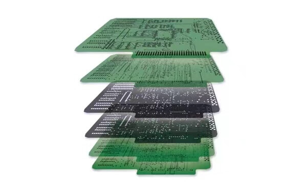
Simply put, PCBA is the finished circuit board formed after the PCB is assembled, SMT process, etc. PCB signal layers are divided into 2, 4, 6 and 8 layers. We are generally 4, 6 layers.
The aforementioned is a succinct summary of the variations between PCB and PCBA. Next, we will briefly introduce the difference between PCBs and PCB assembly.
The main types of PCBs include
Single-Sided PCBs
Single-sided PCBs are the most traditional type of printed circuit board. This circuit board is suitable for simple electronic devices, such as power supplies, led lighting, etc. It has a conductive layer on top of it. The manufacturing process of single-sided PCBs is simple and low cost, especially for low-density designs. When a single-sided pcbs fails, the repair will be relatively simple.
Double-Sided PCBs
The double-sided pcb trial industry to be more extensive, such as sups, cell phone systems, etc. The difference between double-sided PCBs and single-sided is that it adds a layer of conductive layer at the top and bottom. Compared to single-sided, it will be a smaller, more compact circuit. Double-sided PCBs are more flexible in operation. We can use through-hole technology or surface mount technology to mount the circuit.
Multilayer PCBs
Generally, those containing more than two copper layers are called multilayer PCBs. Multilayer PCBs can be used for more advanced electronic devices, such as computers, communications, aerospace, etc. It is intended to be more powerful, more compact, smaller, and typically more flexible.
Rigid PCB
A rigid PCB is a circuit board that cannot fold. A rigid PCB is a robust, inflexible printed circuit board. The board’s substrate is rigid, the rigidity and strength of the board. Their substrate, copper, solder resist adhesives, and heat bond silkscreen layers. Its advantage over other boards is low electronic noise, lightweight, and easy maintenance and diagnosis. However, it cannot modify the shape once the committee is formed.
Flex PCBs
Flexible PCBs are usually made of polyamide, PEEK, or polyester film. The biggest advantage of Flex PCBs is that they can bend them to the shape you need. This makes it ideal for soldering components. And it can also eliminate connectors. Therefore, flexible PCBs are used in many high-temperature and high-density applications.
Rigid-Flex PCBs
Rigid-Flex PCB is a hybrid circuit board. It combines both advantages, allowing narrower conductor lines to take up less space. Rigid-Flex PCBs combine components from both flexible and rigid boards and can be folded and continuously bent. This 3D functionality reduces the need for space.
Halogen-free
This is an environmentally friendly PCB type, which can make into any PCB. Its biggest advantage is that there is no pollution to the environment.
What is PCBA board?
Surface Mount Technology
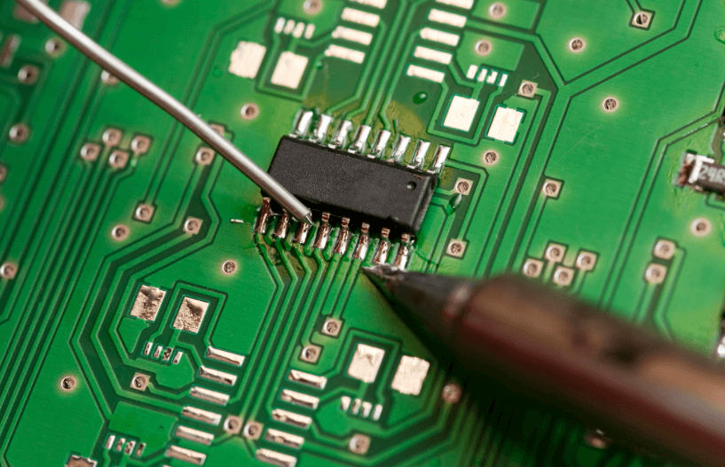
The assembly method known as Surface Mount Technology (SMT) involves attaching electrical components to the surface of a PCB. Higher connection density is possible thanks to its high levels of automation and flexibility. It enables manufacturers to incorporate intricate circuitry into tiny pieces.
The four basic steps of PCBA SMT:
- PCB: The PCBA designer applies solder paste to the PCBs where it is needed.
- Component placement: The assembler then positions the features on the board.
- Reflow soldering: The PCBA board is then heated in a reflow oven by the PCBA designer until the solder paste reaches the temperature necessary for the production of solder joints.
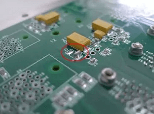
- Inspection: The assembler inspects every step of the SMT process, including before and after flowing and before and after component placement.
Through-Hole Technology
Compared to SMT, it is an older technology. However, it strengthens the bond between the board and the component, making the assembly more robust and dependable.
Fully or partially automatic through-hole assembly is possible. The PCBA through-hole procedure includes the following phases.
Through-hole technology is put together. This process involves drilling holes in the PCB through which can connect electronic components called leads.
- Drilling: The first step in the through-hole process is to drill holes in the circuit board. These holes must size to fit the component leads.
- Placement of leads: The assembler places the tips in the holes.
- Solder: Soldering is the process’ following stage. This step ensures that the assembly is securely fastened in place.
- Inspection: The assembly is continually examined to make sure the PCBA is performing as it should.