
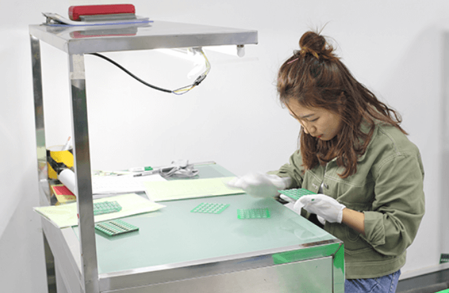
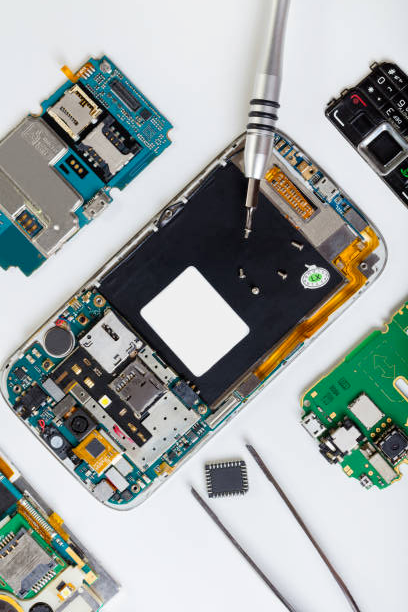
While the manufacturing of anything seems difficult. Often people create a rough idea into basic and general procedures. Though everything revolves around these general principles. But in the backend, a lot is going into detail. That is why you will find people broadly predicting things. However, when you visit any location, there is another schematic process going on. When you hear the name Printed Circuit Board. You will develop the same rough idea regarding its manufacturing.
What is a Multilayer PCBS?
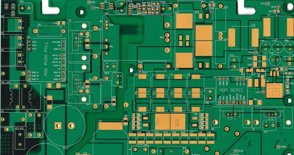
Whether you call it a Multilayer PCBS or by the full name of the Printed Circuit Board, there is no difference. It has a sandwich-like shape that contains two layers. These layers behave as a conductor in addition to insulator. Moreover, the PCB performs two primary functions for any system it goes into. At first, it has to provide suitable space for the components of a system over its surface. In addition, the components find fixation on the surface. Or on the outer layers of the PCB perfectly. Secondly, a Multilayer PCB has to offer a favorable connection. It is between the terminals of the components on its surface. In addition, the connection has to be between the terminals.
Basic Structure
Often you will hear the name of boards rather than surfaces or layers. However, the meanings do not change. These layers of boards consist of conductive patterns of copper. However, these opposite ends have a fine connection with vias. In the Multilayer PCB terminology, vias refer to the holes. These allow connection between the conductive boards and the insulating layer in between. These holes have a see-through shape. This means their cut is complete.
Sizing and Panel
But the production seems more difficult if you consider the singular size alone. Rather, Multilayer PCBS come out from large sheets one at a time. No matter the size you require of the Multilayer PCB, the manufacturers use a single long sheet to do it all. This single sheet, from an engineering perspective, is what we call a panel. From the first step of the manufacturing to the last, the maker considers a single panel until the cutting begins.
Thus, let us begin with the Multilayer PCB manufacturing steps sequentially.
1. Designing
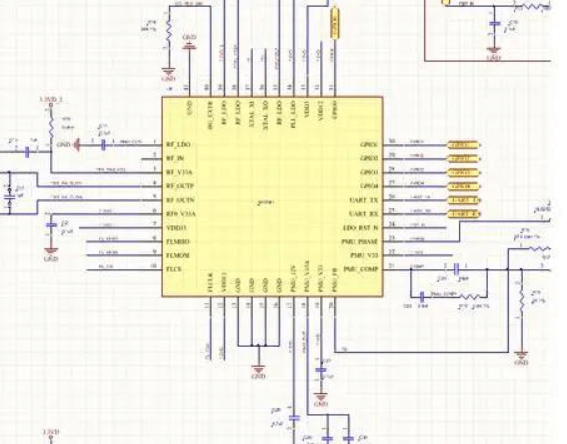
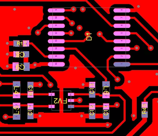
The first step in all sorts of engineering work remains the same. It is to design the structural drawing of the component or element under consideration. Often, the designs seem easy or one-dimensional. But a few components involve a lot in them. For example, a Multilayer PCB structure is not complex but brings design to perfection. At first, you will be drawing a simple design which will then be imported into the CAM software.
The CAM operator has to consider various aspects of the design. For instance, the design has to meet the PCB requirements and rules. It is of importance to produce markings on the design. Moreover, the drill size adjustment, solder mask, silkscreen, and editing layers find correction and verification. Hence, the final design reaches finalization.
2. Photo Plotting
At first, let us consider the basic meaning of photo plotting. The process uses a plotter to implant holes into a sheet. Though the common use of this methodology occurred in old cameras or photo booths. However, there is a selective or unique usage still out now. One common use happens in a Multilayer PCB manufacturing unit too.
In such a unit, a laser photoplotter finds use to produce effective photo tools. These tools help in the processes of solder masking in addition to the silkscreen one. Since the Multilayer PCBSdeals in different layers or boards, the plotter plots a separate film for each layer. The size for each film is around 18×24 inches, while the thickness is not more than 7 mils.
3. Imaging and DES
During Multilayer PCBS manufacturing, the imaging process is of high importance. This process involves the application or transferring of the images. It is like traces onto the Multilayer PCB. The second step is known as Develop/Etch/Strip or DES. The following process involves easing the plating process. For this, the DES has to develop an effective copper pattern which later helps in the plating.
However, the following step involves sub-steps to follow. At first, the dry film application takes place on the panels i.e. of copper. Laser imaging comes into business for imaging the panels. Next, the development of a dry film takes place. In this development, the regions facing exposure remain intact. Whereas the regions that do not face exposure develop off. Anything that is left behind acts as a barrier. This is to prevent the etching of the useful conductive pattern. Thirdly, the etching of the copper that faces the exposure takes place. Finally, we have to strip off the leftover dry film. This is so we have the necessary conducting pattern.
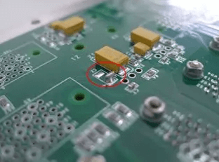
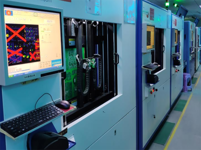
4. Automated Optical Inspection
By inspection, we know that it involves a thorough inspection. But every inspection takes place during the beginning to avoid potential flaws later. And AOI is a method to carefully observe the layers of the Multilayer PCB we want to manufacture. The inspection takes place before the lamination of layers can begin.
The images of the Multilayer PCB from the panel find a comparison. This happens with a standard PCD data set. It becomes easy to determine where copper is abundant or facing a shortage. Either way, the results will not match the ideal requirements. Manufacturers say that if the defects do not show up now. They will never show up during upcoming processes.
5. Black Oxide or Brown Oxide
The general terminology for the process is ‘Oxide’. But the name finds a difference considering the process selection. However, the process finds high importance and great positioning after the AOI. If the AOI is about inspecting the outer surfaces.This process deals with inspection and roughening of the inner layers of the PCB. The reason is to roughen the inner layers so the strength increases. This strength will help to keep the inner layers in a strong lamination bond. Furthermore, if the bond is weak, the proper or required lamination will not find succession.
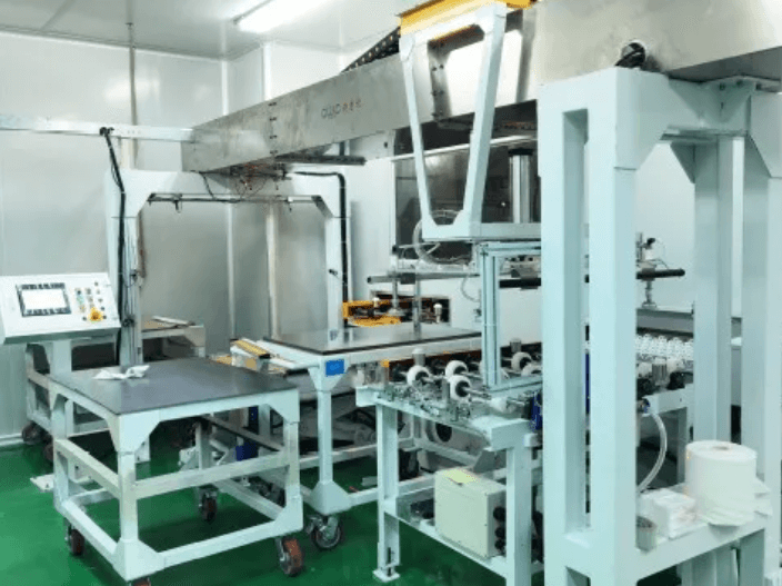
6. Lamination or Joining
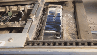
The lamination process involves the joining of two surfaces to each other. Although the lamination process resembles the joining one. But in this specific process, the use of pressure and heat find important. For manufacturing a multilayer printed circuit board with a multi-layer structure, lamination is of utmost importance.
The following process involves the joining of the inner layers of the multilayer printed circuit board material. However, this joining happens at a high temperature and pressure. The equipment that helps in the lamination process is a hydraulic press. The process involves fusing and laminating prepregs, fiberglass. Their lamination happens under the immense heat the hydraulic press induces.
7. Drilling
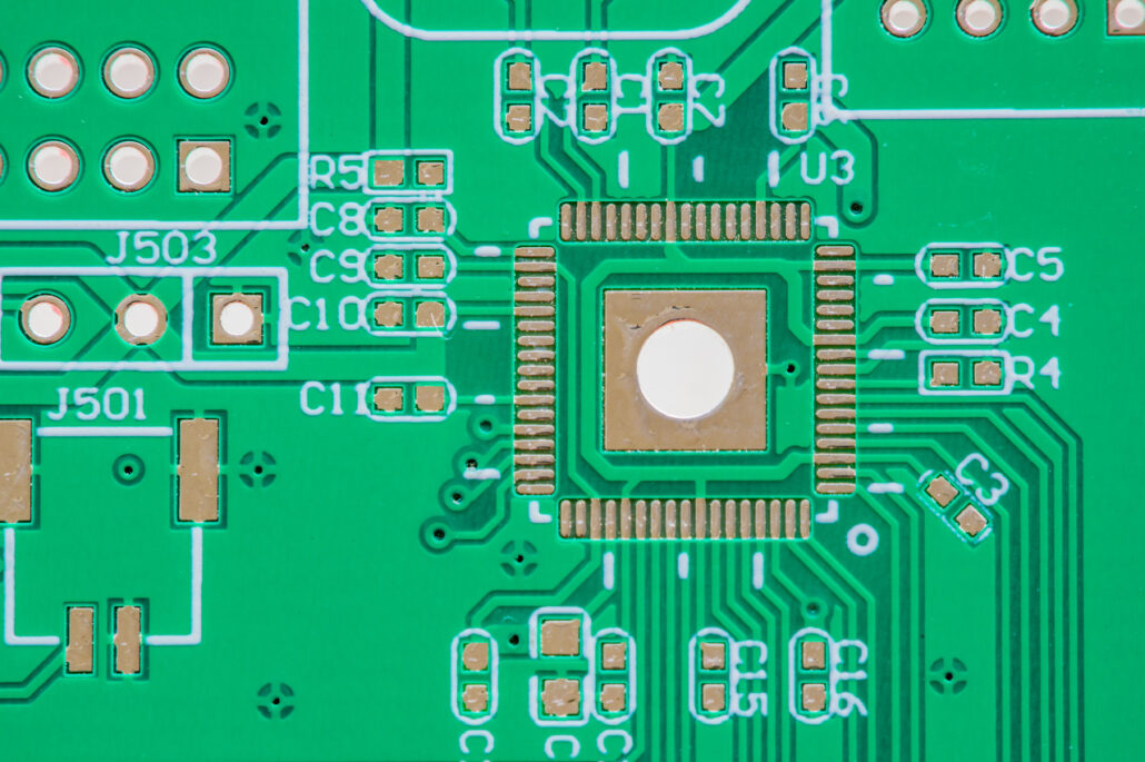
The process of drilling is fun to watch and sometimes difficult to operate. It is because precision and care of great order are the demand. For manufacturing PCBs, there is wide use for producing drill holes. In general, you will require holes to attach and fix multilayer PCBs into useful locations. Whereas for a special purpose, these holes allow connection of the terminal components. In addition, the joining of layers in the multilayer PCB also happens through these holes.
However, cutting them is not straightforward. Rather, the drilling process makes use of a carbide tool. This tool easily removes the chips swiftly from abrasive materials to avoid distortions. Although the manufacturers drill holes through multiple panels at a time. This arrangement mostly depends on the orders.
8. Deposition of Copper
Consider covering anything completely in a matte cover. Although at first, you will mention the exquisite look it gives to the covered item. But only the wiser one will highlight the protection it carries. Although this process does not resemble the protection or merely looks. But it explains the example perfectly.
In the following process or the electroplating process, copper layers find addition. It happens chemically on the surfaces facing exposure on the panels. Moreover, this copper plating also happens in the walls of the holes. That is the holes that result from the drilling. It is to make sure that all the areas of the multilayer PCB have enough copper introduction and covering.
9. Dry Film Application
The following process involves the application of a film on the outer layers of the PCB. In essence, such a process has wide importance. It is because without applying the outer film, electroplating cannot begin. In addition, the following process prepares the panel so the electroplating can begin.
A laminator comes into the business for this. It applies a dry film or an imageable photo on the multilayer circuit board surface. The dry film finds exposure through laser imaging. However, the exposing phenomenon remains similar during multilayer PCB manufacturing. That is, exposed films remain intact until the development of the unexposed one.
10. Copper Plating
In most engineering applications, the plating or electroplating process has great importance. This process follows a set methodology. This is regarding cathodes and their reaction to anodes. The multilayer pcb design requirements include the addition of copper on the conductive patterns. Moreover, the demand is to cover the inside of the holes with copper too.
Thus, to meet the following requirements, the panel is connected to the cathode bar. While the copper acts as an anode in the anode solution. But copper plating is not the only thing of significance. Once the plating ends, another plating i.e. tin plating begins. This second plating helps the etching of the multilayer pcb acting as a barrier.
11. Strip Etch Strip Process
Once we finish with the plating, there comes the process of removal. This removal process involves carrying away the unwanted surfaces and layers. In such a process, the panel goes through three processes stepwise. That is, strip, etch and then strip process. At first, it is the requirement to strip off the dry film resist from the panel.
When this stripping-off finishes. A copper layer exposes off which the tin plating did not cover. Now, the etching process takes place on this copper layer. It leaves behind only a few traces. In addition to the pads around the drilled holes. Moreover, other copper patterns remain intact on the surface. Finally, the tin that remains undergoes the third process or the stripping process. The tin goes away and leaves behind only the leftover copper.
12. Solder Masking
Masking is applied where the critical factor is high. Some conditions and places require you to be extra-protective. Thus, in this case, you look for some covering. In multilayer pcbs, there is a risk that the components might form a bridging. Often, it becomes difficult to break. This bridging also results in the development of electric current during the assembling. To avoid this, the copper surface goes under complete coverage through a solder mask. This mask covers the entire surface of the copper through a strong printing process.
Later, the exposure to UV light begins after which the exposed parts remain. The parts or regions that do not expose go away. The mask then undergoes baking that makes it stiff.
13. Surface Finishing
A good finishing protects the things which are meant for long-lasting. We know that during PCB production, some copper surfaces expose off. Thus, to avoid their oxidation, a good finishing is necessary. The printed circuit board allows different finishes over its surface. The most common one is Hot Air Solder Level.
However, some additional surface finishes include:
- Electroless Nickel Immersion Gold
- Immersion Silver
- Immersion Tin
- Organic Solderability Preservative
- Soft Gold
- Hard Gold
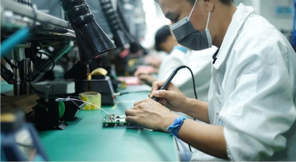
14. Testing and Fabrication
At first, the testing begins on a flying probe tester. This is an electrical test in nature. The test uses electric signals to communicate the result and response. The machine operates using several arms and probes. Thus inspecting different areas of the multilayer printed circuit board surface. The major inspection the device does is to determine spaces or openings. Based on these results, the manufacturer can send them in the trash. Or consider repairing them.
Once the testing finishes and the multilayer circuit board is good to fabricate. The CNC comes into play. A CNC machine lends support to cut required PCBs from a single large panel. Through this device, we obtain different multilayer circuit boards of diverse sizes considering the requirements. Edges involving a bevel or chamfer display also cut out easily through this machine. And we obtain the perfect Multilayer Printed Circuit Board.