
Introduction
Making a PCB layout has evolved through the years. You may have heard of many popular PCB software that came out. Examples of such are Eagle, Cadence-Orcad, Cadence-Allegro, Altium, and Design Spark, to name a few. However, there is a PCB layout software that is popular among the open-source community today. If you’ve heard it right, it’s KiCAD, and this software has taken the engineering community by storm.
What is KiCAD?
KiCAD is a free and open-source PCB layout tool. If you want to avoid paying for software to make a schematic and route your boards, go for KiCAD. Additionally, KiCAD will support you up to the end until you fabricate your boards. How good could that be? Everything you need is in this one-stop, easy-to-use PCB design suite.
Jean-Pierre Charras started the development of KicAD in 1992. After that, KiCAD continued to evolve. The KiCAD project aims to be an open-source PCB Design Suite for beginners and professionals alike.
Though KiCAD is free, donating to the KiCAD project keeps the project going. You can donate before downloading the KiCAD application on the KiCAD website.
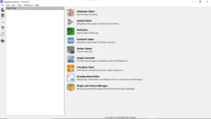
Here are the Capabilities of KiCAD
- Schematic Entry
- Symbol and Footprint Editor
- PCB Layout tool
- Gerber and Assembly Files Generation
- Design Rule Checking
- Gerber Viewer
- 3D Viewer
How to Start a PCB Layout in KiCAD
First, you should download the KiCAD installer from KiCAD’s main website. After that, follow the installation procedure. KiCAD is multiplatform and is available in different operating systems, including Windows, Mac, and Linux.
After installation, you can open KiCAD and run its IDE. You’ll find that it’s straightforward to use and navigate. It has a friendly GUI where you can immediately choose your desired operation through widgets. Alternatively, you can also use the menu on the upper right.
Create a New Project
Before doing the layout, you must create a new project. Click File -> New Project and then name your project. Try not to add spaces on your project’s path and filename to make it compatible with some scripting tools that you may find helpful soon. KiCAD creates a project folder containing everything needed for a PCB design, such as the schematic and board files.
Open the Schematic Editor
- Click Schematic Editor to start your new schematic design. KiCAD has a powerful schematic entry tool that works with a symbol editor to create or edit part symbols. Many symbols and footprints are already saved in KiCAD’s internal library; you don’t have to worry about making each part. However, if you wish to create your part, you can still do it in the Symbol Editor.
- Click the Add a Symbol tool on the right side to insert a symbol. There are plenty of symbols to choose from. Additionally, you can select the part footprint to use. Once you’ve picked up your symbol, place it on the schematic sheet. You can interconnect the parts using the Add a Wire tool. Click the Add a Power symbol to insert power supply symbols, such as VCC or GND.
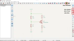
- Edit your part values by double-clicking on the symbols. The later versions of KiCAD automatically assign reference designators to the symbols as you place them. However, you can always edit them or go toTool -> Annotate Schematic to automatically set their values. A fully annotated schematic and parts with complete footprints are critical elements to the next stage of making a PCB layout.
- You can perform a design rule check on your board. Go to Inspect -> Design Rules Checker. DRC will list down the errors you made in your schematic. You can fix them accordingly.
- Click File-> Save to save your schematic. The application will save your schematic file in your project directory.
Open the PCB Editor
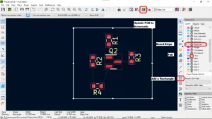
- After finishing your schematic, continue to the PCB Editor from the Schematic Editor by clicking the green icon above. Alternatively, you can select the PCB Editor through the startup IDE. KiCAD has a versatile and easy-to-use PCB Editor. Like the Symbol Editor Editor, the PCB Editor works with the Footprint Editor, packed with hundreds of footprint libraries. These footprints are industry standard.
- The PCB Editor is easy to navigate. Zoom in and out by scrolling through your mouse. Pan the view by right-clicking and then dragging on the PCB editor window.
- Place each footprint of your part symbol from your schematic here. To continue with this operation, click the Update PCB with changes made to schematic icon above.
- Continue to update your PCB if there are no issues encountered. All your part footprints are ready to be placed in the PCB Editor area. Click any part on the PCB Editor window to place them. You’ll see those parts initially compressed and tightly spaced with each other. This presentation is okay because you’ll place them according to your parts placement plan later.
- Before making your parts placement, you have to define your board area. Every PCB needs a board edge or cutout to define this area. This procedure is vital since most PCB manufacturers almost always need this data. To do this, find the Layers tab on the right side pane. Highlight the Edge.Cuts layer. After this, create a rectangle by using the Draw a Rectangle tool. This drawn rectangle is now your board edge. Adjust its size and thickness accordingly.
- Now that you have a board area, you can begin doing parts placement. Click each part to move them to your desired location. While doing placement, you’ll find helpful the Layers tab on the right-hand side. Turn ON or OFF the layers you want and don’t want to use. For example, you can turn off the F.FAB layer to clear out fabrication drawings. You can turn ON or OFF the F.Silkscreen layer to show or hide your reference designators. During placement, you can change any part’s layer (top or bottom) by pressing F (for Flip). The part’s color will change according to your layer color. You can also change the views on your solder paste and mask layers.
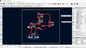
- You can start wiring your board through the Route tracks tool. You can change track widths by pressing Q and add vias by pressing V while wiring. You can also change the layers of your tracks through the Layers tab. KiCAD is versatile and easy to use when doing wiring. You’ll find that the routing tool sometimes predicts your best routing strategy. To create your route without the routing strategy, wire up shorter track lengths first.
- To create a plane (such as a ground plane), use the Add a filled zone tool. Make sure to select the correct net and layer in the dialog window. Create the outline of your plane; upon finishing the last side, right-click, and then choose close track. Connect the pins of the parts needed to connect to this plane and ensure they all have the same net. Vias will also automatically connect to the plane if they have the same net.
- After placing and wiring your components, fix or edit your reference designators. To do this, Turn on the silkscreen layers. Keep your ref des away from solder masks or part edges. It’s not good to have silkscreen ink smother the solder pastes. Also, the operator should see reference designators clearly and comfortably using the board. If needed, place a legend or line pointing your parts to its ref des.
- Like the Schematic Editor, you can do DRC in the PCB Editor. Go to Inspect -> Design Rules Check. Continue running DRC; you may see several issues like disconnected nets, overlapping silkscreen, and floating nets. Fix these issues while scrolling through your design in DRC mode. This DRC tool is crucial because it usually catches design issues hidden from the naked eye.
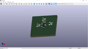
- View your output in 3D. Although KiCAD is free and open source, it has a 3D viewer that most free PCB design software doesn’t have. The details of the 3D view are impressive. Press Alt-3 on your keyboard, and you’ll have your 3D view generated in no time. 3D views help you visualize your boards to foresee any upcoming issues. You can also visualize any chassis problem you may encounter with your board. To navigate your design in 3D, use your mouse’s scroll key to zoom in and out. Click on the left mouse button to tilt your board to certain angles. Use the arrow keys to pan your board. Additionally, there are navigation tools above to ease your operation in 3D.
Conclusion
These are the steps to make a PCB Layout in KiCAD. KiCAD has several components, it has a Schematic Editor, PCB Editor, Symbol Editor, Footprint Editor, Gerber Viewer, and 3D Viewer, to name a few. You can use KiCAD from the beginning of your design by making a schematic. Then proceed to make a PCB layout out of this.