
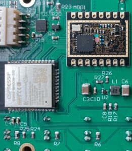
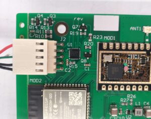
Printed circuit boards (PCB) are essential for operating electrical devices or gadgets such as phones, computers and many other electrical appliances. They basically carry electrical information in the form of bits and transmit it to the required component in order to execute a program. The program therefore performs the task and eventually lets the device to operate.
So printed circuit boards (PCB) are basically the control center of an electric device without them is almost like a car without an engine, they won’t function. My research will focus mainly on the defects, assembly, and ways of fixing circuit boards.
For many high-end, intelligent project operations, Printed circuit board assembly defects can create serious project problems in several ways:
Time to market
The Assembly defects will affect your product’s time to market. Solving any assembly problem takes time, and it takes a whole team to work together.
Cost
Any delay in bringing a product to market will increase the cost of the project, and these defects will often cause the project to go beyond budget.
Performance failure
If a defective PCB has entered the market, it may cause performance failures, as well as safety incidents. All these will affect the brand reputation of the company. The company will recall unqualified products and even bear legal responsibilities, which will affect the promotion of the project and the cost.
To prevent these issues from hurting your company and contributing to long-standing project safety management issues, make sure your team understands the most common PCB assembly defects and how to reduce them.
We can help you with the world’s top guidance in this area. The following is an overview of the most common and harmful PCB assembly defects the team encountered while working on the project..
Bill of material is incorrect
For a professional team ,the BOM (Bill of Materials) must be accurate to prevent delays during assembly. Sometimes, there is incorrect information in the BOM, such as outdated information or a part number that does not match the part assigned to it. In many cases, the parts ordered are too large for the PCB. These errors are often not discovered by professionals until after the parts have been shipped and installed. Therefore, the team should verify that all the information on the BOM is accurate several times before moving forward with the project.
Design for manufacturability errors
DOF is a key element in the design of printed circuit boards. It ‘s common for teams make mistakes in the placement of components. For example, a common problems is that components are too close to each other. If you don’t focus on accurate spacing, your team will find that it can’t automate properly. As a result, your manufacturing team will face some challenges when using pick and place machines.
Welding problem
Solder should be positioned on PCB to ensure structural support of components. For example, companies that use wave soldering should ensure that their rotating parts can enter vertical waves. During wave soldering, placing a taller part behind a shorter part may create a shadow effect, resulting in a reduction in the tensile strength of the solder joints on the pins. There are many other important problems related to this:
1.Logical Deletion
2.Lack of solder resistance layer
3.Provide a limited area for maintenance
1.Logical Deletion
During manufacturing, teams may apply uneven heat during reflow, and components may stand upright at one end without welding the ends down. This problem, called “logical deletion,” is typically caused by different trace widths from the two sections, meaning that the widest trace acts as a radiator. Teams ensuring that heat is conducted evenly throughout the
assembly welding process is the best way to avoid logical removal and all associated component placement problems.
2.Lack of solder resistance layer
In many elaborate PCB design projects, the team may will not use solder resistance layers due to lack of operating space. The lack of a solder resistance layer may result in the formation of a solder bridge when the component is connected to the PCB during assembly. This will cause a lot of problems, good Chinese team will add solder resistance layer on all fine PCB surface.
3.Providing a limited area for maintenance
Repair access is an important consideration when designing PCBS. The product should be designed to allow seamless maintenance or upgrade of the PCB in the future.
Without enough space between components, teams cannot effectively fix systems or build parts. This problem can increase the time required for some upgrades and can easily damage PCB components while technicians make component changes.
7 types of PCB welding defects to be aware of
Let’s face it, welding is hard work. Employees need years of training to become proficient with the correct solder, and even machines are not 100% correct. Inevitably, you will encounter PCB welding defects at some point.
However, by understanding the most common PCB welding defects, you can take steps to avoid them, and you are one step closer to preventing PCB failures.
Common solder defects in printed circuit boards.
Welding defects can occur for a variety of reasons, from operator errors to contaminants. The most costly of and well known of these flaws is :
- 1 Open
- 2 Too much solder
- 3 component shift
- 4 cold joint
- 5 Weld bridge
- 6 webbing and splash
- 7 lift pad
13 Common PCB welding problems that the team can avoid
- 1. Solder bridging
- 2. Too much solder
- 3. Tin ball
- 4. Cold connector
- 5. Overheated connector
- 6. Tombstone
- 7. Insufficient wettability (through hole)
- 8. Insufficient wettability (surface mount)
- 9. Welding jump
- 10. Lifting pads
- 11. Solder shortage
- 12. Solder spattering/webbing
- 13. Pin holes and blow holes
What can we do to avoid welding problems?
Consider the resistance welding design
The solder resistance layer, usually green in color, covers the PCB surface with a thin polymer coating to protect the copper from the environment. At the same time, the solder resistance layer comes in a variety of colors, including green, white, blue, black, red, yellow, etc. The welding resistance layer can protect the circuit, anti corrosion and moisture-proof. In addition to preventing oxidation, they also prevent the formation of tin Bridges, which is also valuable. When the solder does not adhere well to the coating. A barrier layer can be designed between pads to form a barrier layer dam. This is especially useful for chips such as ics and BGA, where the gap between the pads can be as fine as a few thousandths of an inch.
Place reference markers
The reference mark is a circular solder resistance layer opening with a circular bare copper piece in the center that will be placed on the PCB board during the PCB design phase. Components that require special handling are benchmarked by panel benchmark tags and individual components. The pick and place machine treats them as reference points on the PCB in order to align the SMD components on the board. If used properly, the mounting accuracy can be improved. Similarly, poor design of reference marks (e.g., improper placement or insufficient reference points) may result in poor orientation and thus increase the risk of welding problems.
Cooperate with good PCB assembly plants
If manually welding and sourcing components yourself poses too much trouble, or if you are facing problems regarding working tiny components that might prove to be an enigma for the scope of your eyes ability to perceive, then work with a professional PCB assembly company that is experienced and familiar with the pitfalls of PCB assembly. UETPCB offers comprehensive turnkey services, including parts procurement and assembly,etc. Whether you’re prototyping or scaling up to mass production, UETPCB is the perfect partner for smooth and worry-free PCB assembly.
We offer a variety of sponsorship and value-added services to deliver an unparalleled PCB experience designed to minimize failure and maximize productivity and efficiency while supporting developers. We include PCB DFM and PCBA DFA design inspections, as well as free one piece functional tests per PCBA order, and free prototypes for commercial users, and provide services for Raspberry PI, Tesla and many other international enterprises.
Get instant online quotes now and we look forward to sincere working with you.
Selecting a qualified and top level assembly team is the best way to eliminate errors and avoid them
Selecting a qualified and top level assembly team is the best way to eliminate errors and avoid them
To avoid each of the mistakes we highlight, make sure you choose a top level assembly team with at least ten years of experience. Qualified companies can provide precise designs for the seamless manufacturing stage.
Your professional team should have expertise in:
Composition analysis
Comprehensive component inspection is another key factor when working with an electronic technology companies. The partner company shall have the ability to review the power requirements and location of each component to ensure effective heat management. Component experts who understand the market will help you find as many alternatives as possible to PCB parts that can be purchased or easily obtained.
Design for manufacturing
The quality, outstanding companies that work with your company should be able to review your PCB design manufacturing issues. The process involves analyzing the PCB and all components for compatibility, then considering the design dimensions of the board and the welding process to ensure the integrity of the complete structure at each manufacturing stage.
Final inspection of finished products
Prior to mass production of PCBS, designs should be inspected by qualified PCB assembly experts. The outstanding team will use systems such as automated optical detection, which includes the use of professional cameras to detect catastrophic structural failures. The equipment’s professional camera will check for factors such as component position, missing solder and short circuits. When the in-depth analysis is complete, you will have a perfect PCB ready for the market.
The steering circuit center performs PCB assembly in China
We are a professional electronics manufacturing company (PCB manufacturer in China) with more than 15 years of experience in providing professional PCB assembly services. Our products are widely used, Automotive, Medical, Consumer Electronics, Aerospace, Digital Communications, Industrial Control and more. All of us are working hard to produce the most cost-effective printed circuit boards for our customers.