
PCB, or printed circuit board, is the backbone of modern devices. It’s usually used as a base for connecting and arranging electrical parts. It generally comes with different PCB layers. Each layer is responsible for unique tasks. Their flat, rigid bodies make a stable base for placing parts. Their main job is ensuring the electrical connection is safe and efficient.
This article mainly highlights the different types of PCB layers. It shows how they work within a PCB.
What is a PCB Layer?
A PCB board mainly has three layer categories: structural, functional & conductive.
A PCB has different structural layers, such as the substrate, copper, solder mask, and silkscreen. Each layer does a particular job in making the PCB work.
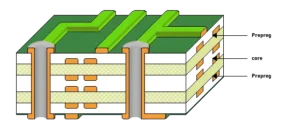
To make a PCB, these layers are stacked together. Adhesives hold them in place. Most important are the copper layers. They sit between the insulating layers. So, a PCB layer is like a separate level in a sandwich.
Regarding conductive layers, the number of PCB layers is typically the number of copper layers in a PCB. Multiple layers are necessary to accommodate complex circuit designs.
However, there are eight different functional layers. We will talk about these layers in the following few sections.
Every layer in a PCB has a unique purpose. The substrate layer makes the PCB strong. Copper helps connect electrical parts. On the other hand, a solder mask protects the trace from damage. Finally, silkscreen helps us know which part is which.
Without these layers, the electronics wouldn’t work right. So, each layer is super important for the PCB to work.
4 Common Structural Printed Circuit Board Layers
As mentioned, each layer in a PCB has a unique purpose. They work together and make the PCB both robust and effective. They protect it from hazardous situations and ensure it works smoothly. However, let’s check them out in detail.
Layer #1 Substrate Layer
The substrate layer is the foundation of a PCB. It provides a sturdy base for all its components. You’ll find it at the bottom of the PCB. It holds all the elements together.
The substrate is usually made of fiberglass (FR4). It is tough and rigid, ensuring the PCB’s stability. Although flexible PCBs may be made of plastic (Kapton), some may use epoxies. However, fiberglass (FR4) is the best for creating high-quality circuit boards.
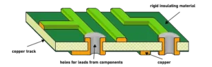
Layer #2 Copper Layer
The copper layer is a thin sheet of copper foil heated and attached to the circuit board. It’s right above the substrate layer. The copper layer is crucial for conducting electricity.
Different PCBs have varying numbers of copper layers. Single-sided PCBs have only one layer of copper and are commonly used in simpler electronic devices.
On the other hand, double-sided ones have copper on both sides. They typically use vias to connect the top and bottom layers. As a result, they can deal with tighter routing of traces. This feature is handy for connecting circuits across the board.
Note that thicker copper layers are prevalent for handling high power.
Layer #3 Solder Mask PCB Layer
The solder mask layer is a protective coating applied to the surface of a PCB. It is typically green in color and covers the copper traces on the PCB. It acts like a shield to prevent the copper traces from touching anything that could cause damage.
Once the copper layer is in place, you can add the solder mask. This layer also insulates the copper, preventing it from contacting other metals.
The solder mask layer is typically made of liquid epoxy resin. For coloration, this liquid comes with a green pigment.
Layer #4 Silkscreen Layer or Overlay Layer
The silkscreen layer, also known as the overlay layer, is found on the outermost layer of the PCB. It contains letters, numbers, and symbols, like labeling on a map.
Silkscreen generally acts as your guide. It shows you which part is which on the PCB. With labels and symbols, it’s easier to know where to connect LEDs or pins.
Single Layer vs Multi-Layer PCBs
A single-layer PCB has only one conductive copper layer. Its design is simpler and cheaper but has limited capabilities. Multi-layer PCBs, on the other hand, have more copper layers. They can handle more complex circuits and components. However, they are more expensive.
Therefore, the choice depends on the project’s complexity and budget.
| Aspect | Single Layer PCB | Multi-Layer PCB |
| Number of Layers | It contains only one conductive copper layer. | It consists of multiple conductive copper layers. |
| Component Density | Lower component density due to limited routing space | Higher component density |
| Size | Often larger to accommodate traces and components. | It can be smaller as components and traces can be distributed across multiple layers. |
| Complexity | Less complex design | More complex design |
| Cost | Generally lower cost | Higher cost |
| Signal Integrity | More susceptible to interference | Better signal integrity |
| Application | Suitable for simple electronic devices | Ideal for complex electronic devices |
Functional Layers on a PCB Board
When you look at the top of a PCB board, you’ll see different layers, each with its unique job. Let’s take a closer look at what they do.
Mechanical Layers
The mechanical layer in a PCB clearly shows the physical structure. It defines precisely the shape and size of the board. Manufacturers use this layer for PCB fabrication and assembly.
Its main job is to ensure the PCB is built correctly and according to the design specifications. In addition, it helps you cut and shape the PCB board during fabrication. However, there are also other layers on top of that. Cutouts, tooling holes, and edges are some other sections that stand out.
Keep Out Layers
Leave my area! Keep-out layers are like boundaries that tell you where you can’t put stuff. They mark areas where you can’t place components or draw wires.
These layers are super helpful because they help you keep electrical items organized. It also enables you to make sure nothing important gets messed up.
Keep-out layers ensure you follow the rules and do not put items where they shouldn’t be. Eventually, they help you make the most efficient use of space on the circuit board.
Routing Layers
Routing layers in a PCB are where copper traces run to connect electronic parts. These layers link components by carrying signals between them. It’s like a road on a map.
Good routing is vital for many reasons. First, it helps signals move smoothly and reduces signal interference. Second, it controls electromagnetic EMI. Finally, it ensures everything works effectively.
Sometimes, complex designs may need multiple routing layers. This is like adding extra lanes on a highway to handle more traffic.
Power and Ground Planes
The power and ground plane is a specific layer in a PCB that carries electricity. Its main job is to ensure the power and ground voltages are appropriately spread across the PCB. In a technical sense, this helps keep the power to the electrical parts stable. It also ensures that the paths for the return of power are smooth.
Power and ground planes effectively spread the heat, which can help cool the board.
Split and Ground Planes
A split plane in a PCB divides the power or ground layer into separate sections, each with its specific voltage level. This can create distinct zones for analog and digital grounds.
The main job of this plane is to isolate different voltage regions. It technically prevents noise interference. However, by carefully dividing the surfaces, it manages noise coupling. They also supply multiple voltage levels needed by various components on the PCB.
Solder Mask Layers
The solder mask layer on a PCB is a protective coating made of insulating materials. In most cases, liquid epoxy resin is used as the PCB solder mask material. This layer covers most parts of the PCB. However, it leaves some areas exposed for soldering.
Its main job is to protect the PCB from oxidation and prevent electrical short circuits. In addition, it helps define areas where electrical connections are made and isolated.
Solder Paste Layers
As the name suggests, this is the layer where you apply the solder paste. Solder paste improves the flow of solder between component leads and PCB pads. As a result, you can get a secure connection for reliable electronic assembly.
Solder paste layers ensure that the solder paste is applied correctly. This layer is crucial for designs that use fine-pitch or small parts. Overall, it ensures that the soldering is done correctly and efficiently during production.
Overlay Layers
The overlay layer is also renowned as the silkscreen layer. It is where important information is printed. It is essential for helping in production and repair tasks.
These layers usually use the solder mask layer as a background and are mostly found on the outer layers of the PCB.
Ensuring the printing lines up correctly with the solder mask layer is essential. So, the overlay layer is like the labels on a map, showing you where everything is on the PCB.
Number of PCB Layers
You can also find various types of PCBs based on different conductive copper layers. The following PCBs are the most common in today’s world.
2 Layer PCB board
A two-layer PCB is also renowned as a double-sided PCB board. It has a single insulating core sandwiched between thin copper layers.
PCB boards with two layers are suitable for low-cost and relatively simpler projects.
4 Layer PCB Board
As the name suggests, a four-layer PCB board has two additional copper layers. The extra room for tracing typically improves signal quality and reduces noise. It also offers higher component density.
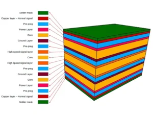
6, 8, 10 & 12 Layer PCB Board Stack up
Accordingly, you may also find multiple-layer PCB board stack-ups. Each type is suitable for unique applications. This diversity generally arises due to distinct needs from various industries. These multi-layer PCB boards are widely used in industrial designs and complex layouts.
| Number of Layers | Layer Configuration |
| 6 Layer PCB Board Stack up | Soldoermask | HS signal layer | Prepeg | HS signal layer | Core | HS signal layer | prepeg | HS signal layer | Core | HS signal layer | pregeg | HS signal layer | Solder mask |
| 8 Layer PCB Board Stack up | Additional two HS signal layer |
| 10 Layer PCB Board Stack up | Additional 4 HS signal layer |
| 12 Layer PCB Board Stack up | Additional 6 HS signal layer |
Contact Us Today
Ready to start your next project? Contact us today for expert PCB design and manufacturing services. Our team is here to assist you every step of the way. Contact us now to discuss your requirements.