
General PCB production will do the full inspection after the completion of two steps: one is the completion of the circuit (inner layer and outer layer); The second is after the finished product.
The way to check the circuit after the inner and outer layer
Electrical measurement
The electrical measurement method is one of the stress testing methods. When the metal resistance wire is subjected to tensile or compressive deformation, the resistance will also change. A resistance strain gauge can be made by winding the resistance wire repeatedly into a special shape (such as a grid).
Before measurement, the resistance strain gauge is pasted on the part to be measured by a special adhesive. When the shell deforms under load, the resistance wire in the resistance strain gauge deforms along with it, resulting in the change of the length and cross-sectional area of the resistance wire, thus causing the change of its resistance value. It can be seen that there is a certain correspondence between the change of resistance and strain.
The corresponding change can be measured using an electrical resistance strain gauge. Using Hooke’s law or other theoretical formulas, stress values can be obtained. During electrical measurement, the factors that produce various measurement errors should be eliminated as far as possible. For example, the deviation of strain gauge position, the tightness of the contact between strain gauge and shell wall, the welding quality between strain gauge and wire, the change of environment and temperature, etc.
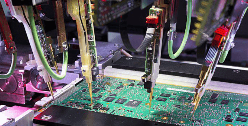
Visual inspection
A magnifying glass with a circular tube to check the quality of the line and alignment accuracy. If the outer hole and coating quality need to be inspected, it is usually further confirmed with a 10x eyepiece. This is a very traditional operation mode, so the demand for manpower is quite large. However, the current high-density design of the board is almost impossible to visual inspection, so AOI will be used a lot.
AOI (Automated Optical Inspection)
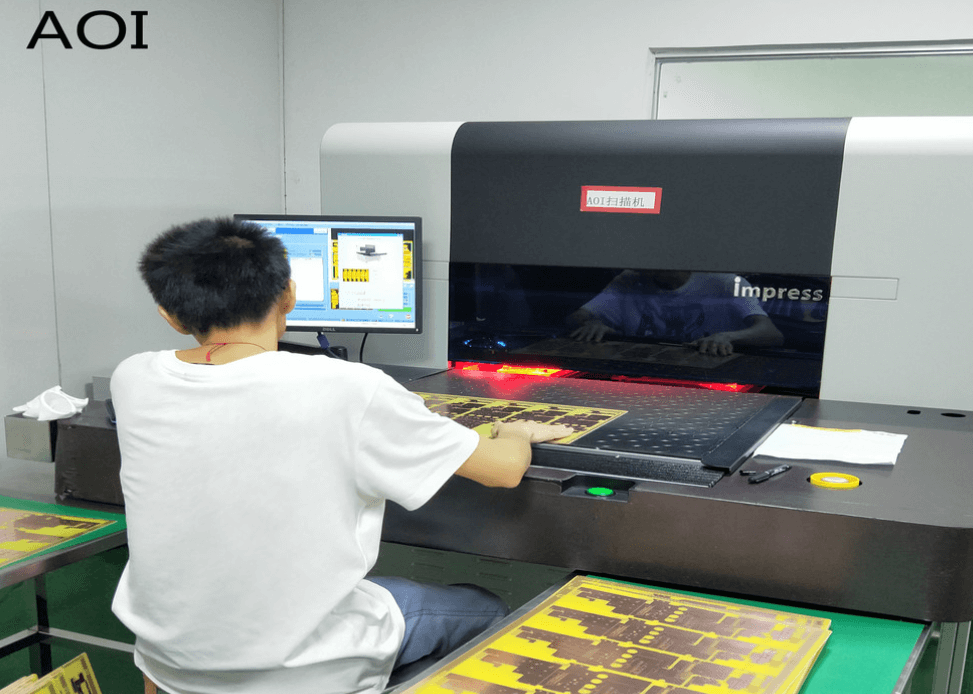
AOI applied range
Signal layer, power layer, after drilling (both inside and outside) Negative film, dry film, copper layer (working film, after dry film development, after circuit completion) At present, most of the applications of AOI are still focused on the detection after the completion of the inner line, but a larger process to replace manpower is the board that has been made surface finish after painting, especially like BGA board, which is small in size, thin in line and large in quantity. The demand for manpower alone is very amazing.
Principle of AOI
The basic principle of AOI is to judge whether the object under test meets the standard by comparing whether there is a large difference between the object under test and the standard image by using image technology. Therefore, the quality of AOI depends on its image resolution, imaging ability, and image discrimination technology. In the early days, AOI was mostly used to inspect defects in the surface printing of IC (integrated circuit) packaging.
As the technology evolved, now it is used in SMT (Surface Mounted Technology) Assembly online to detect the quality of the parts on the circuit board after the Assembly of the solder (PCB Assembly) or check whether the solder paste printing meets the standard. The biggest advantage of AOI is that it can replace the manual visual inspection before and after the SMT furnace, and can judge SMT parts and assembly defects more accurately than human eyes.