
The printed circuit board or PCB is designed in a controlled manner to connect different components in electrical devices. PCBs have different copper layers that are interconnected with each other, which defines the complexity of PCBs. They come in a different number of layers ranging from single and double up to twelve layers. Several layers increase the complexity and functionality of any PCB.
Single-layer and multiple-layer PCBs categorize based on their structure. Both types of PCBs are used in everyday life. The choice between a single-layer and multi-layer PCB must be made before designing a printed circuit board. Many commonplace devices employ both styles of design. Which one is ideal for you will depend on the type of project you are utilizing. Single-layer boards are for simpler devices, whereas multi-layer boards are more typical for complicated devices.
You can guess with the name of both PCBs what the distinction is between both PCBs. Single-layer PCBs only have one base material layer, while multi-layer boards have numerous layers. By thoroughly examining these boards’ designs and operations, you may see several changes in them. Today PCB is used in a wide range of electrical appliances made from one or more insulating layers. Here we will discuss single and multiple-layer PCB in detail.
Single layer PCB:
Many essential electrical gadgets use single-layer PCBs. Single-layer PCBs comprise just one layer. They have a conductor design on one side and components on the other. One layer of conductive material is included on these PCBs. A substrate, a shielding solder layer, conductive metal layers, and a silkscreen make up a single-layer board.
Single-layer PCB has just one layer of conducting material, and the other side utilizes to attach various electronic components to the board. Single-layer PCBs are the essential part of electronics but are still used in many electrical appliances. Double-sided or double-layer PCBs are also available, with both sides fabricated with copper on both upper and bottom sides. Double-layer PCBs are more complex and better than single-layer PCBs.
Pros of single-layer PCB:
There are many advantages of single-layer PCB, as mentioned below;
- Single-layer PCBs are cost-effective and mainly used because of their low-density design.
- Single-layer PCBs are easy to design and manufacture. Drilling, soldering, and re-soldering are easy steps in manufacturing single-layer PCBs.
- Bulk ordering is easy for single-layer PCBs because they are lightweight and easily designed.
- Single-layer PCBs take less time to design, so these are the ideal choice in case of quick PCB orders.
Cons of single-layer PCB:
Although single-layer PCBs are easy to design and manufacture, they have some limitations, as discussed here.
- Some large and complex circuits need more space and connections for components assembling those lack in single layer PCB. That’s why single-layer PCBs are not suitable for large-connection devices.
- Single-layer PCBs also lack enough speed and power to operate many connections.
- It has lower capacity and speed to operate complex functions.
- They are not decisive for major devices that need more power.
Applications of single-layer PCB:
Single-layer PCBs are still the top ones in many devices, but they are primarily used in simple devices to operate a single function. As discussed below, single-layer PCBs have been extensively used in many more superficial and complex machines.
- Single-layer PCBs use in everyday simple electric and manual devices, e.g., radios, mobile phones, calculators, coffee machines, cameras, and printers.
- Single-layer PCBs are standard for storage devices, e.g., solid-state drives with sensors and other power supplies.
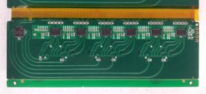
Multi-layer layer PCB:
A multi-layer printed circuit board (PCB) contains more than two layers and at least three conducting copper or conductive material layers. The top and bottom layers of a multi-layer PCB resemble a double-sided PCB, but there are extra layers on both sides of the core. These layers join together by copper-plated holes. The top and bottom layers of the multi-layer PCB are used to mount the active and passive components, and the interior stacked layers mainly use for routing.
Multilayer PBC is one of today’s electrical appliances’ essential parts to improve performance. The substrate and material should be carefully designed and chosen to improve performance.
The first step of manufacturing a multi-layer PCB is to prepare the board design. The next step is to decide inner layer core and then laminate using copper foil sheets. Then apply heat, vacuum, and pressure to make sure that there is no air between layers.
Multi-layer PCBs with a high layer count need thin dielectric, which results in tight coupling between the layers by default. They frequently function better in EMI performance and signal integrity in high-speed electronics. To account for the minimum thickness of the materials used, the board thickness must also increase as the layer thickness does.
Multilayer PCBs comprise two or more insulating layers that are flexible, durable, lightweight, compact, and perform multiple functions. These PCBs are electrical boards used in various industries, e.g., telecommunications, military, and Defense.
An odd and even number of layers is used to design PCB. Designers prefer an even number of layers over an odd number when creating multi-layer PCBs since laminating an odd number of layers might result in a complex circuit and expensive costs. A multi-layer PCB can be manufactured with any number of layers. Smartphones can employ up to twelve layers, whereas some applications need four to eight.
A PCB board substrate that has been properly constructed can effectively lower crosstalk and electromagnetic emissions while also enhancing signal integrity to deliver low inductance power. Compared to double-sided boards, the proper design of multi-layer PCBs can boost immunity to RF fields by ten or more.
Pros of Multi-layer PCB:
Although multi-layer PCBs are advanced and complex and require experts to design them, these have many advantages, as mentioned here.
- Advanced design principles and developing manufacturing techniques apply in multi-layer PCBs to reduce board size while preserving functionality. Multilayer PCBs also use in smartphones and other small-sized electronic devices, so they may be quickly modified to meet the rising demand for electronic wearables.
- Multilayer PCBs are light weighted and effectively used in small gadgets and smartwatches. These are lightweight because of reducing the multiple connections between layers.
- Multilayer PCBs are specially designed to perform multiple functions. They have several features required by smartphones because a single-layer board typically cannot provide them.
- Multilayer PCBs are more durable and flexible because they are specially designed to bear pressure and heat.
- In contrast to using several single-layer PCBs, multi-layer PCBs use to operate on a single connecting point.
Cons of Multi-layer PCB:
As discussed here, there are also many drawbacks to manufacturing and designing multi-layer PCBs.
- Multilayer PCBs are expensive compared to single-layer or double-layer PCBs because of the increased labor and costly machinery used to manufacture them.
- The manufacturing process of multi-layer PCBs is complex as it requires more time and has to follow many rules to design them. These are more often designed according to their applications.
- ·Domain experts must design multi-layer PCBs to follow specific rules and use CAD software.
Applications of Multi-layer PCB:
Multilayer PCBs use day-to-day devices to improve electronics’ performance and efficiency. Multilayer PCBs are widely used today in various electrical appliances, with several layers ranging from four to twelve. Some of the main applications of multi-layer PCBs are discussed here.
- Due to the compact size and multifunctionality of multi-layer PCBs, they are most commonly used in smartwatches and small gadgets.
- Multilayer PCBs use in the telecommunications industry because of their durability and flexibility.
- Multilayer PCBs also extensively utilize in medical devices for the treatment and diagnosis of disease due to their lightweight and multifunctionality.
- Defense and the military also use multi-layer PCBs due to their low weight and compact size.
- Due to withstand extreme conditions, multi-layer PCBs also use in aerospace and automotive systems.
Conclusion:
You need to select PCB according to your demands. You can use a single-layer PCB if you want a cheap and quickly produced PCB suitable for simple devices. It would help if you kept in mind the pros and cons of single-layer PCB e.g., cost, time, high volume, and simple design will give you an advantage but this is not suitable for more complex and powerful devices as it has lower power and speeds as compared to multi-layer PCBs. Suppose you need to operate a more complex and more extensive project. In that case, you must go for a multi-layer PCB as it is more powerful, durable, flexible, multifunctional, has a single connection point, and is lightweight. However, multi-layer PCBs will be costly, require more complicated designs and repairs, and require more production time. That’s why they are limited.