
Something You Need to Know About PCB Vias
A circuit board is made up of layers of copper foil. The different layers of the circuit are connected by a hole (VIA). The purpose of the circuit board is to conduct electricity, so it is called a through hole.
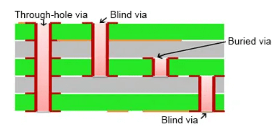
Types of PCB vias
Plating Through Hole (PTH):
This is the most common type of through hole, which runs through the entire circuit board and can be used for internal interconnection or as mounting holes for components. The process is simple and the production is easy so the cost is low.
Blind Via Hole (BVH):
Blind holes are located on the top and bottom surfaces of the printed circuit board and connect the surface circuit of the PCB with the inner circuit. They are called “blind holes” because they cannot see the opposite side. The production process is complicated and the drilling cost is high.
Buried Via Hole (BVH):
A connection hole located in the inner layer of a printed circuit board. Any circuit layer inside the PCB is connected but not connected to the outer layer. Production is difficult, so the cost is much higher than “through hole” and “blind hole”.
Design rules for PCB vias
1. The hole cannot be designed on the pad.
2. There should be no holes in the 1.5mm outward extension area between the metal shell of the component and the PCB.
3. No holes designed in the assembly adhesives coating area.
4. To save cost, it is recommended not to design blind/buried holes when BGA is over 0.65mm. 5. The spacing between holes is generally required to be 0.5mm or above, otherwise, holes are easy to be broken in the production process.
PCB vias designed in a common PCB Vs high-speed PCB
PCB vias in common PCB
In common PCB design, the parasitic capacitance and inductance through holes have little influence on PCB design. For 1-4 layers PCB design, 0.36mm/0.61mm/1.02mm (drilling/pad /power isolation zone) through holes are generally preferred. Some special requirements for signal cables (such as power cables, ground cables, and clock cables) can be selected through holes of 0.41mm, 0.81mm, or 1.32mm, or other sizes as required.
PCB vias in high-speed PCB
In high-speed PCB and multilayer boards, the connection of signals also needs to be transmitted from one interconnect to another through holes.
1. Reasonable design of hole size. For some high-density/high-speed PCBs, 0.20mm/0.46mm/0.86mm (drilling/pad/Power Isolation zone) holes can be used.
2. Power isolation area need designed as larger as possible, generally D1=D2+0.41;
3Try to design the signal routing on same layer to reduce the generation of holes;
4. The thinner the PCB board thickness is, the more beneficial it is to reduce the two parasitic parameters of the hole;
5. To reduce impedance, the lead between the hole and the pin should be as short as possible.
6. Add some ground holes near the signal change layer hole to provide a short distance loop for the signal.
7. In high-speed PCB design, to reduce the problems caused by the hole, the hole length is generally controlled within 2.0mm. For holes with a hole length greater than 2.0 mm, the impedance continuity can be improved to a certain extent by increasing the hole diameter. When the hole length is 1.0 mm or less, the optimal hole diameter is 0.20 mm ~ 0.30 mm.
Start your PCB vias fabrication and PCB assembly service in UETPCB
UETPCB has over 10years experience in PCB fabrication and PCB assembly service, highly specialized in 1-48layers PCB fabrication, from through hole in common PCB to blind/buried holes in high-density/high-speed PCBs and HDI PCBs. We can provide custom PCB prototype service to small volume PCB manufacturing, to meet all of your PCB and PCB assembly needs.
Freely contact us to help you out.