
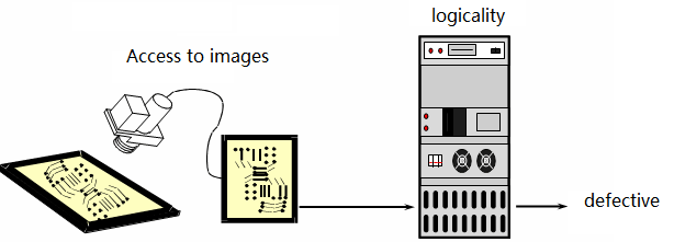
Working principle of AOI detector testing
Application of AOI in SMT processing in a variety of forms, but its basic principle is the same (as shown in Picture 1), the analyte with optical instruments for graphics, usually by sensors (cameras) to obtain the test figure like lighting and digitization, and in some way to compare, analysis, testing and judgment, the equivalent of the artificial visual inspection, automatic and intelligent test.
Picture 1, Schematic diagram of AOI basic Principles
The algorithm of AOI
AOI analysis and judgment algorithms can be divided into two types: design rule test (vector analysis) and graphic recognition test.
Vector analysis according to some given rules to detects graphs. for example, The all traces should be the end of solder points, and all traces width and spacing shall not be less than a specified value and match rules to detect PCB circuit graphics. Picture 2 is a test image of solder paste bridge based on this method. After extracting the digital image of solder paste on PCB, judge whether the solder paste is a bridge connection based on the form of solder paste in the interval area of the solder pads. If the solder paste shape measured according to a certain sensitivity exceeds the preset warning line, it is considered a bridge connection. DRC method has the characteristics of algorithm-based guarantee of the correctness of the tested graphics, easy manufacturing of the corresponding AOI system, easy realization of high-speed processing of algorithm logic, small amount of program editing and small data space. However, this method has poor ability to determine the boundary, so it is often necessary to design a specific method to confirm the boundary position.
Picture 2, Detect to solder paste bridge connection image
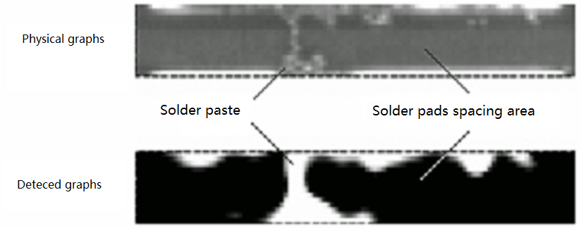
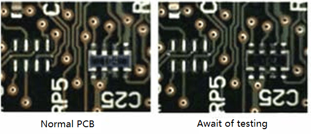
Image comparison is to compare the digital image stored in AOI system with the actual detection image, so as to obtain the detection result. For example, when PCB circuit is detected, the test file (standard digital image) and the test file (actual digital image) are first established according to a normal PCB or computer aided design model for comparison. Picture 3, shows the quality inspection of the assembled PCB using this principle. The detection accuracy of this method depends on the standard image, resolution and the detection program used, which can obtain higher detection accuracy, but it has the characteristics of large amount of data acquisition and high requirement of real-time data processing. The graphic recognition method has obvious practical advantages by replacing the design principle in vector analysis with the design data.
Picture 3, Image recognition and contrast detection
Application of AOI in SMT process
In SMT, AOI is mainly used in paste printing inspection, component inspection, and component inspection after soldering. The emphasis is also different in the detection of different links.
1) There are many kinds of soldering defects, which can be divided into insufficient solder paste on the solder pads and excessive solder paste; the middle part of large solder pad missing solder paste, solder paste too much on the edge part of small solder pad; printing offset, bridge connection and contamination, etc. The causes of these defects include poor rheological property of solder paste, improper machining of stencil thickness and hole annular, unreasonable setting of printing machine parameters, low precision, improper selection of scraper material and hardness, and poor quality, etc. AOI can effectively monitor the printing quality of solder paste and analyze the quantity and type of defects, so as to improve the printing process. This function partially overlaps with SPI, but AOI inspection of solder paste depth is not as good as SPI and the accuracy is low, so UETPCB using SPI to conduct solder paste printing quality inspection.
2) Component placement has a high requirement for equipment precision, and the common defects include missing, wrong, deviation, and opposite polarity, etc. AOI testing can detect the above defects and at the same time check the solder paste on the pads connected to the tight spacing and BGA components.
3) After reflow soldering, AOI can detect components missing, offset and skew, as well as all polarity defects, as well as solder joint correctness and defects such as insufficient solder paste, soldering short circuits and warped feet.
Although AOI is more efficient than manual detection, the results are obtained through image acquisition and analysis and processing, and the relevant software technology of image analysis and processing has not yet reached the level of human brain. Therefore, in some special cases in actual use, it is inevitable for AOI to misjudge or miss judgment. The existing problems in the use of AOI are as follows:
- a) Many paste, little paste, deviation, skew process requirements standard definition is different, easy to lead to misjudgment.
- b) The capacitor value is different, but the size and color are the same.
- c) The correct of polarity judgment is greatly different due to different silkscreen processing methods.
- d) Most of AOI understanding of bad soldering is ambiguous, resulting in hard of judgment.
- e) There are problems in the detection of shielding ring and shielding point
- f) The soldering quality of BGA, FC and other flip-chip components is difficult to detection.
- g) Most AOI programs are complex, tedious and take a long time to adjust, which is not suitable for scientific research units, small OEM factories, production units of multi-specification and small-batch products.
- h) The detection speed of most AOI products is slow, and a few AOI products using scanning method are faster, but the misjudgment and missing judgment rate are higher.