
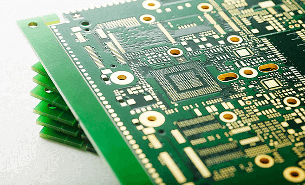
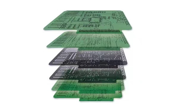
What is 6 layer PCB?
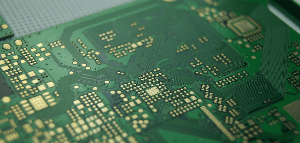
The number of PCB layers refers to the number of copper layers, 6 layer pcb means there are 6 copper circuit layers. It has a compact component layout and reduces manufacturing costs. Usually, electronic and cost-effective products use it. 6 Layers Printed Circuit Board is the same as 3 layer and 4 layer pcb. Both are multilayer pcb.
6 layer board = standard 4-layer pcb + two additional signal layers.
Therefore, a standard 1.6mm 6 layer PCB board stack = top + bottom + 3 Prepreg layers + 2 internal wiring layers + 1 internal ground layer + 1 internal power layer + 2 core layers.
Benefits of 6 layer pcb stackup
6 layer pcb stackup can reduce space and make pcb more flexible. And it also allows for more complex designs. The following list of the various advantages of it.
Smaller size:
Due to PCBs stickup, 6 layer PCBs are smaller and more flexible for the same function. At the same time, 6-layer PCBs are manufactured using lightweight components, which reduces the total weight of these PCBs. Therefore, 6 layer pcb is ideal for many high-tech products.
More powerful:
This multilayer PCB has a very simple layout board. This facilitates a higher transmission speed of electronic devices.
Longer life:
Multilayer PCB stacking protects the inner circuit board from external influences. Multilayer PCBs use multiple insulation layers between the circuits. Protective materials and various adhesives are used to bond these layers. This reduces the loss of the circuit board and extends its life.
Reduced radiation:
A perfect PCB lamination design minimizes equipment radiation, especially in the laminated design of high-frequency and high-speed circuit boards. In addition, if the impedance design is not reasonable, it is easy to cause more significant EMI radiation than standard PCB.
Low cost:
Excellent multilayer PCB stacking design can also reduce manufacturing costs by placing multiple circuits on the same board. And 6-layer PCB stacking makes the connection process on various machines very simple. This simple design helps save space and materials that may be wasted when building large appliances.
Effective signal crosstalk reduction:
A good PCB stack can alleviate impedance differences and signal crosstalk problems.
Factors that determine the design of 6 layer pcb stackup
If done incorrectly or with faults, the PCB lamination design procedure might result in pcb manufacturing failure. As a result, there are some things to think about as you go through the design process.
- Design configuration: It would help decide how you will construct the pcb stackup. You can choose from a variety of 6 layer pcb stackup combinations. The needs of your application determine these settings.
- Electrical Specifications: It’s crucial to think about how much current the 6-layer PCB will carry at any one time. This aids in establishing the right signal path and routing for the draft.
- Design and Production Costs: Must consider the cost of producing a 6 layer PCB stackup. Creating PCB stacks will cost more if the designs are more sophisticated.
- Electrical Specifications: Because the stack is ideal for applications with varying temperature needs, you must consider all areas of thermal identification or specifications while developing a 6 layer PCB stackup.
- Component Density: It’s crucial to think about the type and amount of components installed on the PCB stackup, as this will help with electrical connections.
Application of 6 layer PCB


As the demand for electronic devices grows, so does the demand for multilayer circuit boards from many manufacturers. The following are some of the applications for which you can use 6 layer PCB lamination.
- Consumer electronic devices: such as cell phones, refrigerators, computers, ovens, etc.
- Communication facilities: such as GPS, satellite, etc.
- Medical devices: such as X-ray machines and infrared lamps, etc.
- Transportation: such as cars, airplanes, high-speed rail, etc.
What are the steps for 6 layer PCB design?
- Edit the diagram: Double-check the schematic after you’ve finished creating it.
- Make a new PCB file and establish the 6-layer PCB layer structure as follows: You can import the schematic netlist into the PCB file for 6-layer PCB fabrication after creating a new one.
- Layout: In 6-layer PCB manufacturing, the primary premise of layout is good partitioning. Separating analog and digital devices can also help to prevent interference. Anti-interference is particularly necessary because the digital signal generates much disturbance.
- Grounding layer fabrication: There are two grounding layers on a 6 layer PCB: AGND and DGND. The two are normally separated and found on the second and fourth levels, respectively. Because pads can generate capacitive effects and increase interference, the connection technique uses as few.
- Make the power supply layer: The power supply layer must be divided because multilayer PCB boards have more than one operational voltage value.
- Wiring: Make sure the power and ground layers are in good shape and that the important high-speed signal lines are routed to the inner signal layer.
- Perform a DRC check: For 6 layer PCB production, this step is critical. The PCB drawing must be verified after it is finished.
4 layer vs 6 layer pcb cost
UETPCB is a reputable Chinese 6 layer pcb manufacturer. We offer pcb prototyping at a low cost, high quality, and quick turnaround. We also have 4 layer pcb machines for fast 4 layer pcb manufacturing. PCB assembly prototyping allows you to swiftly test your stack and design, uncover mistakes and flaws in real time, and decrease losses before mass production.
Factors affecting 4 layer vs 6 layer pcb cost.
1. Number of PCB layers.
In general, the same area of the PCB cost will increase with the number of layers. So, in general 4 layer pcb cost will be lower. Generally, 4 to 6 layers will increase the cost by 30% to 40%.
2. PCB size
The same number of layers of pcb, the smaller the size of the cost will also be lower. The cost of producing pcb by 4 layer pcb machine will be relatively low.
3. Manufacturing difficulty
pcb also has many minimum manufacturing parameters. We should try to stay away from the minimum parameters. Because some of the parameters are smaller will lead to lower yields, resulting in increased costs. The same does not recommend using HDI blind holes because the processing of blind holes is much more complex than through holes, which will increase the production cost of PCB.
4. The size of the holes on the board
The board’s size and the number of holes will affect the final production cost. For example, if you need very thin holes, they will also require specialized tooling to produce. In this regard, the size of the holes on the board (design) is the most critical determinant.
5. PCB materials.
There are many classifications of PCB boards, such as RF4, aluminum substrate, epoxy glass fiber board, etc. There is a big gap between the different materials processing. So try to choose the board that can meet the design requirements.
6. 6 layer pcb stackup surface treatment type
The finish you choose for your 6 layer pcb stackup design will affect the cost. Some finishes are higher grade or provide a longer shelf life so that the cost price will increase accordingly.
- HASL, OSP, LFHASL: provide better solderability
- IMM Ag: provides better solderability and Al (aluminum) wire bonding
- IMM Sn: provides solderability
- ENIG: Provides solderability, Al wire bonding, and contact surface
- ENEPIG: better contact surface, Al wire bonding, and solderability
- Elec Au: is an aluminum and gold (Au) wire bond better solderability and contact surface
Conclusion
You should have a lot of knowledge about PCB design by now. 6 layer pcb or 4 layer pcb manufacturing plays a crucial role in the success of electronic devices. It provides you with the best power and flexibility to easily create stack types for your designs.
We ensure that we can make boards of various thicknesses to meet the various requirements of our customers. 6 layer pcb manufacturer professionals will give the best solutions to avoid any problems in the previous stages. We are the 6 layer pcb manufacturer you can trust.