
It is well known that there is a high demand for heavy copper PCBs in the electronics industry. We also know that copper is one of the main components of any PCB. In other words, copper pcb holds a high position in electronics development nowadays. We will use this technology for higher current levels of circuits. In general, usually, pcb copper thickness is about 35μm. When the pcb copper thickness used in PCB is between 100 and 400μm, we call it heavy copper PCB. Below we will introduce copper PCB and its benefits in detail.
Why use copper for PCB alignment?
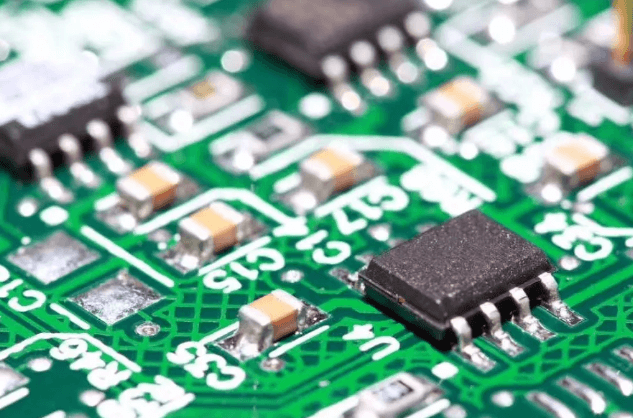
Multiple layers make up printed circuit boards (PCBs), including substrates, alignments, solder resist layers and screen printing. The alignments are one of the most important aspects. This is because they transport electrical impulses to various components on the board. The PCB will not function without alignments. Almost all gadgets that send data will not work without PCBs!
Copper is the most prevalent element used to manufacture alignments today. The heavy copper layer enables a PCB cross-section with high current loads and aids heat dissipation because PCBs are intended for high current output and thermal management. Besides this reason, do you know any other factors that make copper popular in the PCB industry?
How are copper PCBs made?
Glass fiber is commonly used as a base layer on standard printed circuit boards. While this material performs admirably under normal circumstances, it is frequently damaged in high-power applications. For high-temperature applications, switching to a metalcore circuit board, such as a copper-core PCB, provides the endurance and conductivity required. Metalcore PCBs include copper core PCBs. These PCBs have a multilayer design with a copper substrate for superior thermal conductivity.
- Substrate: The substrate is comprised of copper, which has excellent thermal conductivity and heat transmission properties.
- Insulation Layer: Copper core PCBs use prepreg or other highly thermally conductive insulating layers to increase heat transfer.
- Circuit Layer: The circuit layer is made out of copper foil that weighs between 1 and 10 ounces.
- Dielectric Layer: The additional dielectric layer absorbs the heat generated by the circuit layer and disperses it to the copper substrate.
Advantages of Copper PCB
Copper will improve the performance of your board in a variety of ways. Metal PCBs have many advantages over traditional boards. It can not only carry more current, but it can also dissipate heat more effectively.
-
High thermal conductivity
Copper has high thermal conductivity, and the higher the conductivity, the stronger the heat transfer and dissipation. In environments involving high temperatures, standard PCBs, such as FR-4 boards, may not be able to withstand the high temperatures, resulting in extensive damage. Copper PCBs can avoid this problem and extend their life. At the same time, they can support extreme currents, higher temperatures, and frequencies under repeated thermal cycling.
-
Non-polluting
As a completely natural material, copper is 100% recyclable. Using copper core panels will make your project more environmentally friendly.
Durability
Copper core PCBs are less prone to warp or corrode over time due to their better heat dissipation. As a result, copper base pcbs are more durable than ceramic or fiberglass-based boards. Copper base PCBs are also more tolerant of manufacture than ordinary materials, lowering the risk of breaking during development and every day use. -
Compact structure
The package size of heavy copper pcbs is more compact and more suitable for high precision devices. Also, heavy copper pcbs can pass a high current and is suitable for transferring heat to an external heat sink.
Copper pcbs application
Heavy copper pcb is becoming increasingly popular due to all of the benefits and performance mentioned above advantages. Copper base pcb can use in a variety of industries, including medical, military, aerospace, and electrical. Copper clad pcbs have a long service life and can help electronic devices to be smaller.
In a nutshell, the need for copper clad pcbs is driven by two key factors: reliable performance and excellent heat management. Heavy copper PCBs aid in the effective dissipation of heat, ensuring maximum circuit performance. This is why, despite their high cost, Heavy copper PCBs are still in high demand.
Copper pcb possible application products include.
- Lighting: LED street lights, intelligent lights, Christmas lights, etc.
- Transportation: Power controllers, displays, and chips for other smart devices
- Communication: Filtering devices and high-frequency amplifiers
- Computers: Power supply devices and CPUs
- Power supplies: converters, inverters, etc.
- Medical equipment: ECG machines, defibrillators, etc.
Best heavy copper pcbs manufacturers --UETPCB
UETPCB is one of the most experienced PCB and PCB assembly manufacturers in China. We are able to produce the highest quality heavy copper PCB products. We will do our best to produce the highest quality circuit boards to meet your requirements. Check our capabilities in the following table.
| Feature | Capability |
|---|---|
| Material | FR-4 Standard Tg 140°C, FR4-High Tg 170°C |
| Min. Hole Size | 10mil |
| Max Outer Layer Copper Weight (Finished) | 15oz |
| Max Inner Layer Copper Weight | 12oz |
| PCB copper thickness | 0.4 – 10mm |
| Copper surface finish | HASL lead free, Immersion gold, OSP, Hard Gold, Immersion Silver, Enepig |
| Solder Mask | Yellow,Green, White, Black, Red, Blue, etc |
| Silkscreen | Black, White |
| Via Process | Tenting Vias, Plugged Vias, Vias not covered |
| Testing | A.O.I. testing and Fly Probe Testing (Free) |
| Build time | 4-7days |
| Lead time | 1-3 days |