
IoT chip to the module, the whole process of R&D and production
The development of the Internet of Things and smart home has deepened the connection and interaction between people and things, making our lives more colourful, more convenient and more closely connected. The connection of people and things (equipment) depends on the Internet wireless network wireless connection, but the connection protocol is a lot of categories, such as the major WiFi, BLE, ZigBee, Z-Wave, NB-IoT, Lora, etc. And for the WiFi protocol, a number of chip platforms such as Qualcomm QCA4004, MTK MT7688, LEXIN ESP8266, RTL8710 and so on; In this way, it will inevitably bring trouble to engineers in the early stage of product development: what protocol is suitable for the product? What parameters are needed to measure? What are the means of measurement?
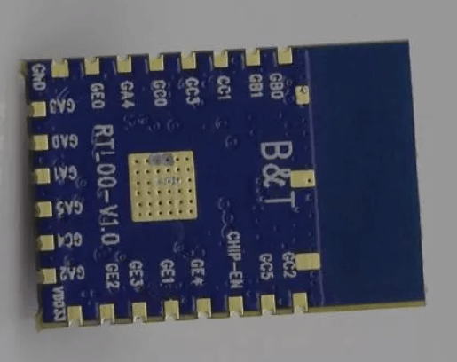
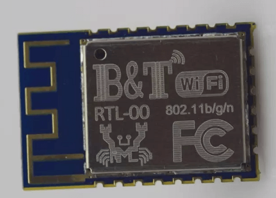
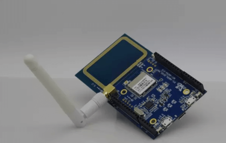
Today with the Realtek RTL8710 WiFi module as an example, from the selection, production process, research and development, PCB production, chip packages and PCB Assembly (SMT) process to give you a detailed explanation.
The four stages from chip to module:
- Chips
- Module R&D
- Module production
- Secondary development support
Chip
Module R&D
It mainly involves hardware design and software design.
We need to consider these aspects, such as scheme selection, schematic diagram and layout design, PCB board and PCBA prototyping, index debugging and parameter testing. Among them, scheme selection is the most important.
1.Scheme selection
The core is to meet the function, easy supply and production, price matching
(1) Demand analysis
Function consideration: the networking mode of WiFi, one-to-one or one-to-many. Terminal products take one to one, used in gateways and routing is one too many.
In the transmission rate, shunt quantity class, control class, if the module is applied in the intelligent home appliance control, select partial control class chip, such as ESP8266, if used in such products as routers, it is necessary to choose flow class chips, such as MTK 7620;
In terms of a functional interface, module developers may consider more the number of chip interfaces, functional support, such as GPIO interface, SPI Flash interface, I2C interface; In fact, this is easy to understand. For example, RTL8710, the WIFI chip of the Internet of Things, has more than 20 GPIOs and supports more input and output devices, or more external connections or controls. Also, the consideration of interface functions cannot be ignored. For example, some of the interfaces of this chip can automatically reduce the power consumption to the lowest state when it is not working, and automatically wake up from the sleep mode when it is in the working state, which can greatly reduce the power consumption of the product.
In addition, in the aspect of the application function, the developer can choose the chip scheme of passthrough or non-passthrough according to the need.
(2) Advantages and disadvantages analysis
In addition to the analysis of the market demand for chip solutions, module developers also need to consider the cost performance and stability of the chip, as well as the original factory and supply channels;
A good product even if all aspects are excellent, but the price is too high for the market, so absolutely no one dares to choose. Of course, we can not only look at the price, as the saying goes, but cheap goods are also very reasonable. If the advantages of the two chips scheme difference are obvious, but the advantage of the chip scheme even if the price is a little higher cannot stop everyone to choose. This is especially critical when it comes to the stability of chip solutions. If it is high power consumption is easy to cause heat and crash chips, how do you let product developers, consumers choose? Of course, heat could be one of the many factors that cause instability, such as chip manufacturers’ inadequate optimization of software code, which can also cause these problems.
The chip solutions offered by different manufacturers or brands may vary. In the chip industry, there seems to be a consensus that the chip solutions of Europe and the United States are preferred, followed by those of Japan and South Korea, and then Taiwan, and finally the chip solutions of the mainland are chosen. Of course, this is on the premise that the price difference of the chip solutions is not large. The module chip solution we mentioned above comes from a Taiwanese manufacturer.
Finally, no matter how good the chip solution, the supply channel is an unstable, or frequent shortage, which is also very fatal for module developers.
2.Schematic diagram design
After the module developer chooses a good chip scheme, it is necessary to develop and design the module. The first thing is to design the schematic diagram.
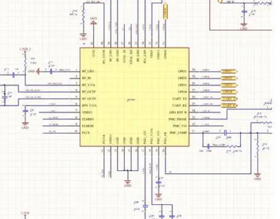
Stability: the developer needs to design the schematic diagram with high stability according to the chip information provided by the chip manufacturer and the specification requirements.
Cost advantage: there are many design options for schematics, but cost considerations should not be ignored. For example, two layers circuit board design, four layers circuit board design can be used, four layers circuit board is also better, but the price is more expensive. This is only one aspect of cost considerations, of course.
Compatible design: the EMC design consideration in schematic design is to consider that the module can still coordinate and work effectively in various electromagnetic environments. The purpose is to ensure that the module can not only suppress all kinds of external interference so that the module can work properly in a specific electromagnetic environment, but also reduce the electromagnetic interference of the module itself to other electronic equipment. EMC design concerns the stability and performance of the whole module.
Difficulty degree of mass production: schematic design should also consider whether it is convenient to process in the future, and good processing means less processing costs. If the design of the schematic resulting in the actual processing of a low rate of goodwill also causes an increase in costs.
3. PCB LAYOUT
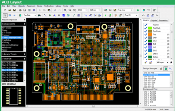
The schematic design of the above part, together with the drawing of the PCB board, is collectively referred to as PCB Layout. Both are complementary, schematic design is to be reflected in the drawing of the PCB board, schematic diagram to consider the drawing of the PCB board also need to consider, and the drawing of the PCB board also need to consider more. For example, RF considerations, stability considerations, structural considerations, and even drawing PCB board also need to consider the aesthetics of the board. Because from the drawing on the board you can see the module manufacturer is not professional in the end.
Of course, according to the PCB Layout, the PCB selection involved, the type and quantity of resistor, capacitor and other materials will be reflected in the BOM (Bill of Material) list of materials. Also, PCB and PCB Assembly (SMT) production will be determined according to this list of materials.
4. PCB prototype
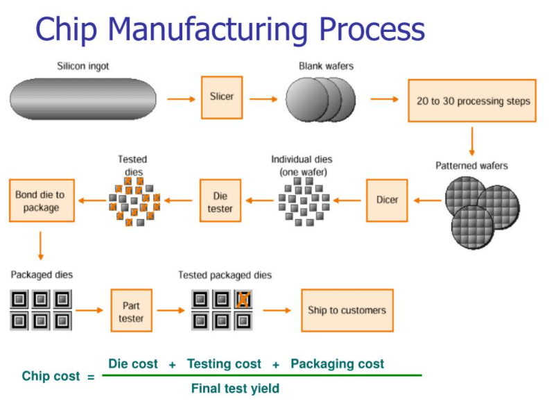
Printed Circuit boards (PCB), or chips, are made of epoxy glass resin and have a different number of signal layers to which chips and other components are soldered.
Vendor selection: For PCB prototype, module manufacturers, if they look for external manufacturers, usually need to consider whether these manufacturers have PCB prototype experience, whether the equipment of the manufacturer meets the needs and the management of the manufacturer is good, and so on.
Process requirements: if the PCB is multi-layers, it is necessary to find a manufacturer who specializes in multi-layers PCB.
5. PCBA prototype
CircuitBoard +Assembly (PCBA) is a PCB bare board that goes through the SMT process and the DIP plug-in process. PCBA is also known as a finished PCB.
PCB & PCBA prototyping is the best choice to verify the quality and performance of a design before starting full mass production. It’s very important to work with a reliable prototype manufacturer who can fabricate the sample boards fast and correct them if you need some printed circuit boards. These boards can rapidly test and verify the designs if any mistakes or potential defects in the early stages of your projects, also order small-quantity prototype runs first is more cost-effective. Our UETPCB offers quick-turn PCB prototype services for PCB manufacturing and assembly at high quality and low cost.
6. Debugging
For the module debugging mainly lies in the hardware circuit debugging and software debugging.
The RF part of general Wi-Fi products is composed of several parts, and the dotted blue box is uniformly regarded as the power amplifier part. Wireless Transceiver (Radio Transceiver) is generally one of the core devices of a design. In addition to the close relationship with the Radiofrequency circuit, it is generally related to the CPU. Here we only pay attention to some of the content related to the Radiofrequency circuit. When a signal is transmitted, the transceiver itself will directly output a weak radio frequency signal with a small Power to a Power Amplifier (PA), which is then radiated into space through a transmitter /receive switch through an Antenna. When receiving the signal, the antenna will sense the electromagnetic signal in the space, and then send it to the Low Noise Amplifier (LNA) for amplification, so that the amplified signal can be directly sent to the transceiver for processing and demodulation.
Hardware debugging mainly involves RF circuit and function circuit debugging. RF debugging includes two major aspects: sending and receiving, in which sending includes sending power, phase error debugging, etc., receiving includes sensitivity, receiving electricity equality. The functional circuit debugging is more related to the specific circuit debugging of a hardware function module.
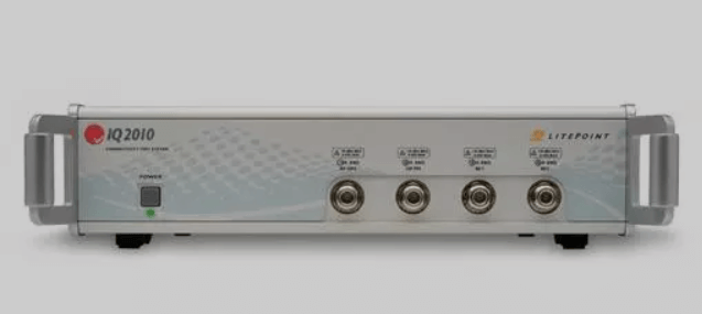
For the debugging of RF parameters, the transmitting TX is mainly Power Power, error vector amplitude EVM, and frequency offset FREQ. In terms of receiving Rx, it is mainly about receiving Sensitivity and Sensitivity. These parameters affect whether WiFi data signal transmission is stable. Special equipment is needed to test it. Such as LitePointd IQ2010, the WT-200.
In addition, the software debugging mainly lies in the stability, the integrity of the function debugging. Generally speaking, specific tuning is performed on a single or partial function, and the next step is to conduct more comprehensive testing.
7.Test
The electronic circuit test is to achieve the circuit design indicators for the purpose of a series of measurement, judgment, adjustment, re-measurement of the repeated process.
Functional test: according to the features, operation description and user scheme supported by the module, test the features and operable behaviour of the module to determine whether it meets the design requirements.
Performance test: it mainly involves testing each functional circuit of the module, as well as signal transmission distance and other parameters.
Stability test: the actual transmission rate, actual power consumption, throughput, wireless connection and other stability aspects of the involved modules are tested.
Burn-in test: It is a test to determine the life of the module and to achieve the best results during use. As the system is in the working state for a long time, it carries on the load operation to each device when it is working. As long as the performance stability of the equipment can be guaranteed under these conditions, the service life of the working module will be longer under the normal environment.
Certification test: some products must be certified by the relevant country designated certification bodies, obtain relevant certificates and add certification marks, can be a factory, import, sales and use in business service places, especially communication products, and international more popular certification such as FCC, CE, RoHS, UL, etc.
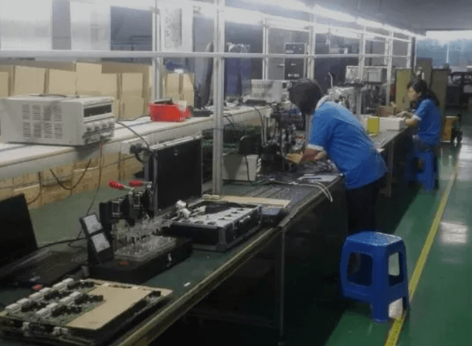
Module Production
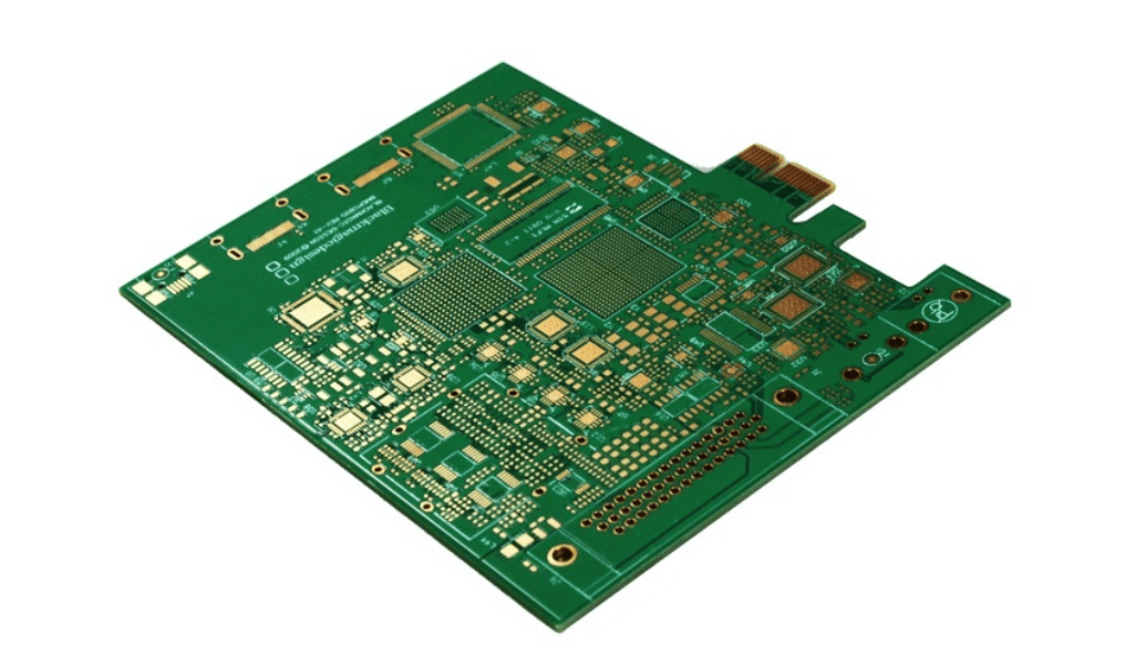
Module production mainly includes PCB production, PCBA(SMT)processing and testing.
PCB production is the most basic and important step of module production. The whole process is shown in the following figure.
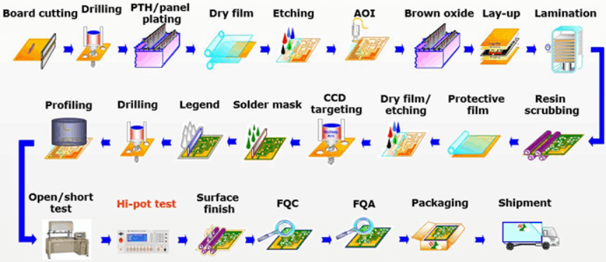
PCB bare board fabricated as design
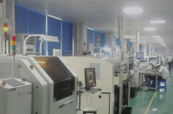
PCB assembly (SMT) processing
According to the PCB characteristics of the module, is mounted on a single side.
Single side assembly process
Incoming material detection → Solder paste printing→ Soldering → Reflow→ Cleaning→ Testing
(1) Material checking: before production, SMT materials shall be checked according to the specifications and quantities of materials according to the BOM and production orders;
(2) adjusting machine: at the same time, the SMT should be programmed and adjusted. After the completion of the adjusting machine, it is the feeding process.
(3) Solder paste printing: apply the solder paste evenly on the solder pads of PCB to ensure good electrical connection between the pins of components and the pads corresponding to PCB during reflow soldering.
(4) Soldering: PCB printed with solder paste and transmitted to the SMT machine by an automatic feeder. The program of the SMT machine is prepared in advance. When the machine recognizes that there is a board, it will start to automatically take material for mounting.
Assembled RTL8710 module
(5) visual inspection before reflow: or called intermediate inspection, it is necessary to pay attention to the polarity of the components, no offset, no short circuit, no fewer pieces, etc.
(6) Reflow soldering: the checked PCB will be automatically soldered after reflow soldering.
At this point, the module production process is basically over.
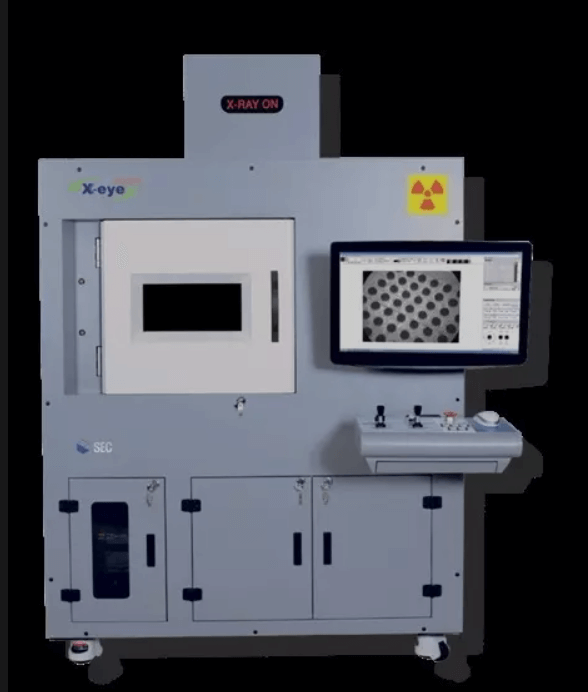
(7) inspection after reflow: here is the main inspection is the appearance to see whether there is bad soldering, tin beads, short circuit, component offset, and so on. Appearance inspection methods are AOI inspection /X-Ray sampling inspection, visual inspection.
(8) AOI test
Normally AOI inspection can be placed before or after reflow, but most manufacturers choose AOI checking after reflow because this is where all assembly errors encountered can be found.
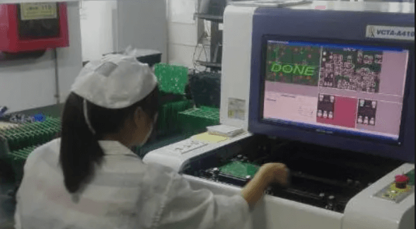
Due to the misjudgment (blind spot, less tin, etc.) rate of AOI automatic optical detection, artificial visual inspection is needed after AOI detection.
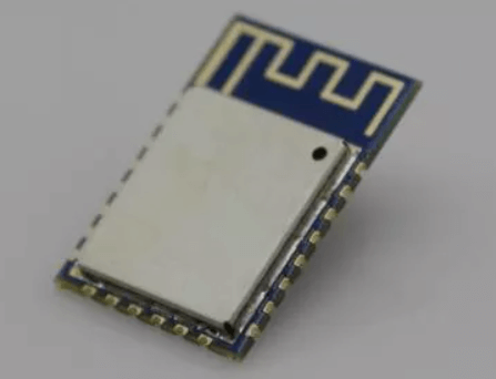
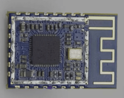
Metal shield cover on the surface of module
However, AOI detection is not feasible for blocks with metal shielding moulds on the surface, so we can adopt another X-ray spot inspection. X-Ray contactless 3D inspection method, when the circuit board layer number is more, the inner layer of the accuracy of the demand will be higher. It can also be used for perspective observation and measurement of the position and shape of the encapsulated objects, and even for the perspective of metal shielding devices.
visual inspection is to first scan the whole board with the eye and then examine the defective areas with the microscope, such as missing tin, short circuit, which can be easily detected by tilting the board to adjust the best vision. It is usually less time to examine irregularities with the eye than to examine them bit by bit with a microscope. Of course, when the problem is found, a microscope can be used for more detailed examination.
Then we use the laser marking machine to mark the module. Through the marking text on the module, we can connect to some chip manufacturers, series, models and other information
Module test
(1) Programming
Universal serial programmer for programming, the first use of random parallel port data line, the programmer and the computer parallel port connection, online programming.
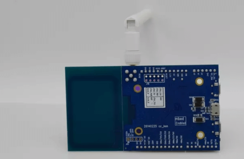
(2) GPIO test special test of GPIO port is carried out through the proprietary test fixture. Place the module on a specially designed needle bed fixture, make the fixture test probe contact with the lead of the component, and check whether the GPIO interface is qualified by checking the LED brightness around the fixture.
GPIO test
(3) Receiving and transmitting power test IQ 2010 tester is used to test the transmitting power and receiving the power of module WIFI.
(4) OthersAfter the test is completed, the module should be packaged before leaving the factory. Module packaging in addition to the general resistance to extrusion, vibration vacuum foam bags, more important and waterproof, anti-static packaging measures.
Secondary development support
Commonly used in intelligent household, industrial control products of WiFi module for embedded normally, different areas, different products, different engineers for the second time development, will encounter some technical problems, more or fewer module manufacturers normally with the developer community, technical hotline, E-mail, instant messaging, on-site support services.
From the demand analysis before the module research and development to the determination of scheme selection, from the schematic design to the drawing of PCB board, from the module hardware and software matching to confirm BOM materials; PCB production, SMT processing and testing related to module production; From module delivery to after-sale technical support, every step is crucial and we can know how important of the PCB and PCBA manufacturers.
Union Electronic Technology offers all the advantages of PCB manufacturing, turnkey PCB assembly service and full box build service with fast turnaround times and an affordable budget. Our primary mission is to continually provide high-quality PCB &PCB Assembly services that make us the best choice for your electronic manufacturing, so welcome to contact us for your electronic products.