
Nowadays, the demand for electronic PCBA hardware terminal customers for electronic contract manufacturing services is increasingly strong. The traditional PCBA manufacturers, due to weak supply capacity, lack of price advantage, unstable supply, and low labor efficiency, lead to low conversion rate and face the problems of fewer and fewer customers. However, in the process of choosing a PCBA OEM factory, the manufacturing terminal factories are faced with problems such as difficulty in confirming the authenticity of materials, unstable PCB procurement cycle, failure of electronic components, maintenance difficulties, and financial risks.
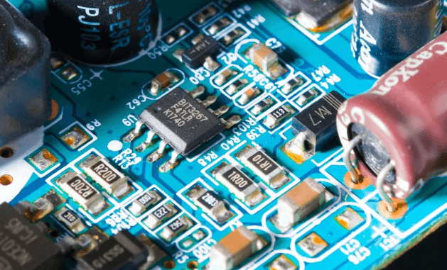
Next, we will collect and share the MLCC failure problems and detection methods in the PCBA assembly and PCB soldering process, starting from the optimization of production process and design improvement, finally to achieve the high reliability of MLCC assembly and soldering.MLCC (Lamellar Multilayer Ceramic Capacitor) is internally composed of multiple capacitors misplaced and stacked, MLCC for short. It has the advantages of small size, large capacitance per unit volume, little influence on performance by environmental factors such as temperature, etc., and is widely used in military communication, radar, artillery fuze, aviation, aerospace, weapon system, and other fields.
MLCC has now become one of the most commonly used components in electronic circuits. On the surface, MLCC looks very simple, but in many cases, the design engineers or production, process personnel on the understanding of MLCC is not enough. Some companies in the application of MLCC will also have some misunderstandings, thinking that MLCC is a very simple component, so the process requirements are not high. In fact, MLCC is a very fragile component, must be careful in PCB assembly process.
Common failures of multi-layer Ceramic Capacitors (MLCC) are summarized and classified as follows: Dielectric breakdown, open circuit, electrical parameter change (capacitance out of tolerance, loss Angle tangent value increase, insulation resistance decline or leakage current rise, etc.), lead corrosion or fracture, insulator rupture or surface arc, etc. Tantalum electrolytic capacitor – voltage overload breakdown and burn out; Surge voltage impact leakage current increases; Polar reverse short circuit; Insufficient high temperature reduction failure; Aluminum electrolytic capacitor — leakage current increases breakdown; Polar reverse short circuit; Insufficient high temperature reduction failure; Organic film capacitors – thermal shock failure; Excessive parasitic inductance affects the realization of high frequency circuit function;
MLCC (Class 2) — Improper SMT process leads to fracture or insulation failure; The poor temperature characteristic of Y5V leads to circuit failure;MLCC (Class 1) — RF design selection matching.
MLCC failure is caused by a variety of reasons, various MLCC materials, structure, manufacturing process, performance and use environment are not the same, the failure mechanism is not the same. According to the analysis of past failure samples, the common failure mechanisms include internal delamination, dielectric defects, metal ion migration, dielectric aging, etc. The same failure mode has multiple failure mechanisms, and the same failure mechanism can produce multiple failure modes, which are not a one-to-one correspondence.
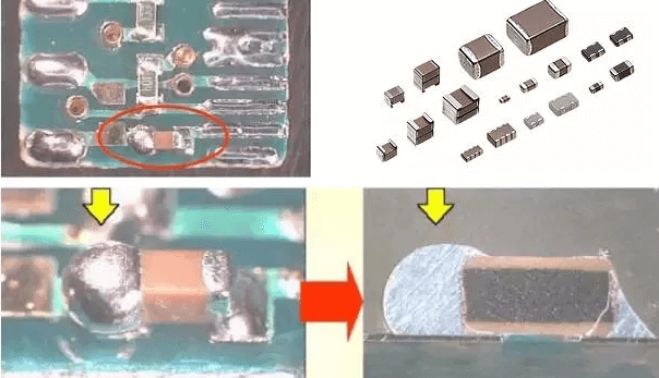
MLCC breakage
Here are some problems in MLCC application, failure detection methods, and matters needing attention.
With the continuous development of technology, patch capacitor MLCC can now be hundreds or even thousands of layers, each layer is micron thickness. So a little deformation is easy to crack it. In addition, the same material, size, and pressure resistance of the patch capacitor MLCC, the higher the capacity, the more layers, each layer is thinner, so the more prone to fracture.
On the other hand, with the same material, capacity, and voltage resistance, small capacitors require thinner dielectric layers, leading to more easily broken. The harm of crack is leakage of electricity, which can cause safety problems such as dislocation of short circuits between internal layers. And the crack has a very troublesome problem is that sometimes it is relatively hidden, it may not be found in the factory inspection of electronic equipment, and it is not officially exposed until the client’s end. Therefore, it is of great significance to prevent the patch capacitor MLCC from cracking.
Analysis of MLCC failure causes and improvement measures
Under normal use of the product, the root cause of failure is the existence of various micro defects such as cracks, holes, delamination and so on outside or inside MLCC. These defects directly affect the electrical performance and reliability of MLCC products and bring serious hidden trouble to product quality.
External factors: cracks
- Thermal CrackIt is mainly caused by temperature shock during welding, especially during wave soldering. Improper repair is also an important cause of temperature shock crack.
When the patch capacitance MLCC is subjected to temperature shock, it is easy to crack from the welding end. In this regard, small capacitors are relatively better than large capacitors. The principle is that the heat conduction of large capacitors does not reach the whole capacitor so quickly. Therefore, the temperature difference between different points of the capacitor body is large, so the expansion size is different, and the stress is generated. For the same reason, that thick glasses are more likely to crack than thin ones when poured into boiling water. In addition, during the cooling process of the patch capacitor MLCC after welding, the expansion coefficient of the patch capacitor MLCC and PCB are different, which causes stress and leads to cracks. To avoid this problem, a good weld temperature profile is required during reflow. This failure is greatly increased if wave soldering is used instead of reflow soldering.
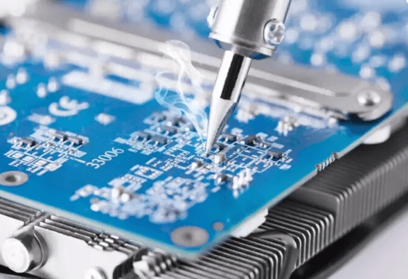
MLCC is to avoid the soldering manual. However,soldering by hand is sometimes unavoidable. For example, for PCB outsourced processing of electronic manufacturers, some products are very small, the manufacturers are not willing to accept this, only manual soldering. When we start with sample orders, it is generally soldering by hand. Rework or repair under special circumstances must be manually soldering; When repairmen repair capacitors, they also soldered them by hand. When manual soldering of MLCC is unavoidable, great attention should be paid to the soldering process.
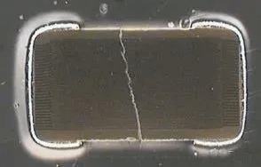
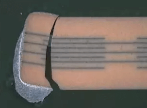
- Mechanical stress Crack (Flex Crack)MLCC multilayer ceramic capacitors are characterized by their ability to withstand high compressive stress but poor bending resistance. Any operation that may cause bending deformation during device assembly may cause device cracking.
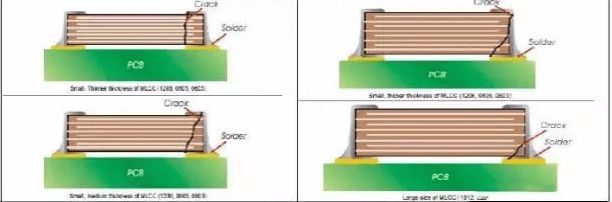
Common stress sources are the process of circuit board assembly operation; Factors such as people, equipment, and gravity in the process of circulation; Through hole component insertion; Circuit test, PCBA board split (V-cut or milling); PCB installation; Screw installation, etc. Such cracks generally originate from the upper and lower metallization ends of the device and propagate to the device interior along with the Angle of 45℃. This type of defect is also the type of defect that actually happens the most.
Mechanical stress factors:(1) the test probe causes the PCB to be bend;(2) the bending over PCB and the rupture impact on PCB;
(3) the suction nozzle is mounted (the pressure of the suction nozzle is too large and the pressure distance is too deep) and the fixed jaw causes impact; When the product is mounted on the printed circuit board, it should not be subjected to too much impact. The suction head and positioning claw must be inspected, repaired, and replaced regularly.
(4) too much solder paste cause bending and cracking of PCB board (such as a shared pad).
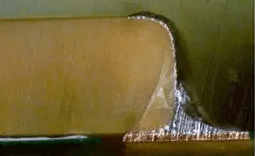
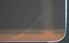
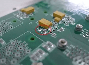
(5) PCB manual soldering: the process of soldering iron head or anti-static tweezers pressing the device body and the two ends of the device solder amount is too much or uneven, can cause cracking, as shown in below picture.
(6) PCBA cleaning process: the cleaning method is wrong or the cleaning brush head is too hard, which can cause cracking; If the device has internal cracks in the previous process, MLCC may cause the electrode and ceramic body to fall off during the cleaning process.
Mechanical stress crack generation principle:
The ceramic body of MLCC is a brittle material, if the PCB is bent, it will be subjected to a certain mechanical stress impact. Bending cracks occur when the stress exceeds the MLCC porcelain strength. Therefore, cracks caused by this bending only appear after soldering.
1)When the PCB board is bent, the stress at different positions is different: the component assembly is close to the point of the PCBA splitter.
Internal factors: voids, cracks, delamination
- VOIDS
The main factors leading to cavity are organic or inorganic pollution in ceramic powder and improper control of the sintering process. The generation of the cavity is easy to lead to leakage, and leakage leads to local heat in the device, which further reduces the insulation performance of ceramic medium and leads to the increase of leakage. This process occurs in cycles and deteriorates continuously. In serious cases, it will lead to cracking, explosion and even combustion of multilayer ceramic capacitors.
- Firing Crack
Sintering cracks usually originate at one electrode and propagate in a vertical direction. The main reason is related to the cooling rate in the sintering process, and the crack and damage are similar to the cavity.
- Delamination
Multilayer Ceramic Capacitors (MLCC) are sintered to multilayer materials by stacking co-firing. The sintering temperature can be as high as 1000℃ or more. Poor interlayer bonding force, internal pollutants volatilization during sintering and improper sintering process control may lead to delamination. Delamination, similar to cavity and crack, is an important inherent defect of multilayer ceramic capacitors.
Improvement of reflow (SMT) process
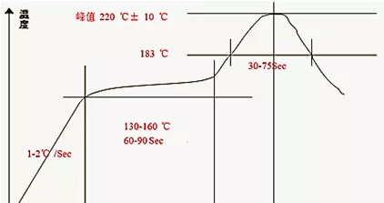
More consideration should be given to the temperature characteristics and size of MLCC in the process selection to avoid defects caused by thermal stress. For example, large-size MLCC above 1210 is not suitable for wave soldering when selecting soldering procedures, because large-size capacitor thermal conductivity design is inferior to small-size capacitor thermal conductivity design, and it is easy to cause uneven heating of capacitor, resulting in destructive stress. Once the soldering method is determined as wave soldering or reflow soldering, attention should be paid to the temperature curve setting of the equipment, and the temperature curve should be set, verified, modified and published by authorized process technicians. In the parameter setting, the jumping temperature should not be greater than 150℃, the temperature change should not be greater than 2℃/ second, the preheating time should be more than 2 minutes, the welding cannot take auxiliary cooling equipment, should be natural with the furnace temperature cooling.
MLCC failure detection method
For external defects, manual visual inspection under a microscope or automatic appearance sorting equipment is usually used. Internal minor defects have always been one of the difficulties in MLCC detection, which seriously affects the reliability of the product, but it is difficult to find. The ultrasonic flaw detection method can detect the internal defects of MLCC more accurately so that defective products can be sorted out and the breakdown voltage and high voltage reliability of MLCC can be improved.
The penetration and reflection (surface wave and bottom wave) characteristics of ultrasonic waves are used to detect defects in objects. By ultrasonic flaw detector to accurately find out the defective MLCC production internal micro defects, and can determine the location of the defect, further analysis of the grinding, for found that internal defects of products, adopt the whole batch of scrap processing, show that the ultrasonic testing method in the detection of internal defects in MLCC, decide on the validity and reliability.
Normal sample: the overall color of the scanning photo of the sample is green-yellow, indicating that the sample body displays normally. The red and blue color on the edge of some samples is caused by the uneven height of the sample edge surface, which is a normal phenomenon. Abnormal sample: the color of the sample body will appear red and blue, then the suspicious sample will be scanned again for confirmation.
The image of the ultrasonic scanning
Failure analysis of other components and chips
Failure analysis is not only for MLCC but also for other electronic components and ICs. The production and use of electronic components failure analysis of product all have the vital significance, through the analysis of process waste defective, early failure, test, test failure, and the failure samples, confirm the failure mode analysis, failure mechanism, clear the failure reason, the prevention countermeasures are provided, to reduce or avoid the failure happen again.
Common IC failure modes
Failure modes: electrostatic damage, metal electromigration, chip bonding failure, over-electrical stress loss, mental fatigue, thermal stress, electromigration failure, physical damage, plastic packaging failure, lead bonding failure.
- Electrical characteristics testing: usually used in the initial phase of failure analysis, the purpose is to understand the electrical parameters of the sample or the functional failure status, to facilitate preparation for further analysis.
- Observation measurement: by observing the external/internal appearance & structure of IC, confirm the abnormal location and specific conditions of IC. This type of test is typically used in conjunction with DPA, or destructive physical analysis.
- DPA destructive test: through liquid erosion, mechanical damage, laser cutting, and other damage methods, the specific failure position inside the IC is located and presented.
- Reliability test: it is to verify IC life and performance stability by using various environmental test equipment to simulate high temperature, low temperature, high temperature, high humidity, and temperature changes in the climate environment.
Conclusion: MLCC is a new type of electronic component, is one of the essential components of electronic information products; It is widely used in various circuits of various military and civil electronic products. Therefore, MLCC assembly and welding quality control are particularly important. So the reliability of the product is not only designed, but also produced, and inspection can only verify the reliability of the product, cannot improve the reliability of the product; Product design, production technology, and process control are the three basic ways to achieve high reliability MLCC assembly.