
Electric appliances or electric boards are always very much controversial and it is very much important that one needs to understand all about it before working on it. There are many things that come into the mind of a person before working on it.
The biggest concern that most people face is that. What are the components in which PCBs are made? What is the exact working of PCB boards? In what categories the multilayer PCB boards are divided?
Do you want to know more about the PCB boards, then the above post is very much beneficial for you. Today, here in this post, we will share all about the PCB boards in detail. So, let’s have a look at the information below:
How are multilayer PCBs made
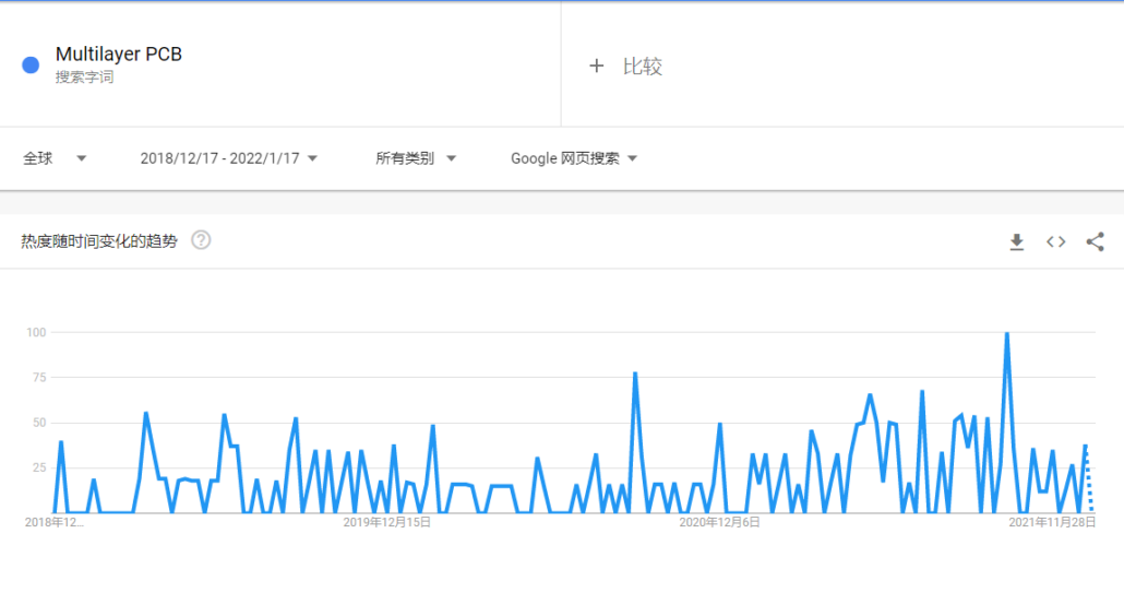
The above image is from the data analysis of Google Trends. We can see that multilayer PCBs popularity is somewhat cyclical. And the heat of multilayer pcb is also increasing so far in rushing 2018.
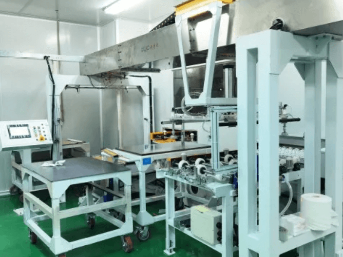
Now coming to our major topic that how multilayer PCBs are made. The layers of multilayer PCBs are connected with the help of high temperature, together they all produce multilayer PCB. While putting pressure on the layers, the makers or engineers always ensure that there is no trapped in between the layers. Guides are totally epitomized by tar, and the glue that holds the layers together are appropriately liquefied and restored. The scope of material blends is broad from fundamental epoxy glass to fascinating clay or Teflon materials.
Issues with the construction of multilayer PCB
But the construction of the multilayer PCB is not easy as it involves many issues, and here we are adding all the problems in detail. We believe that you must understand all its issues while you are going to get all its information.
Delamination
The problem of Delamination occurs when copper gets detached. It can be possible on the internal layers or on the surface. It is a problem, which can be fixed if there is no as such irreparable damage to the board does not occur. For multi-facet sheets, there are more potential regions where delamination can occur. For this situation, the board will, in all likelihood, have to respin.
Layer Alignment
As the multilayer PCBs have multiple layers to align, therefore the chances of getting the layers misaligned get increased. But this does happen along with the single layer or double layer PCBs. Even though the layers get stacks in these multilayer PCBs. To make sure that the electricity must get passed through these layers properly, it must be checked that the layers must be positioned properly.
Drilling Precision
Drilling precision is also the biggest problem while working on multilayer PCBs. While working on it, the alignment must be made simultaneously. Notwithstanding, the base layer of these stacks will normally have a bigger diversion, or the opening will be bigger than the inward layers. This can represent an issue as a bigger annular ring measurement might be important for the bigger diversion.
Via Selection
Another significant issue when building multi-facet sheets is the best through choice. Your decision of vias impacts your board construct. For instance, visually impaired and covered vias require more noteworthy accuracy than through-openings. Part bundles that have fine contributed and require using cushion vias can likewise be risky for a few agreement makers (CMs).
Advantages and disadvantages of multilayer PCBs
Now, coming to the major question: What are the advantages and disadvantages of using a multilayer printed circuit board. If you are looking for it, then you must crack all the information below:
There are many advantages of multilayer PCBs, which all start from technology usage to personal usage, and here we are going to share all the information with you.
Lightweight
Being lightweight, which makes the multi layer PCB to be used for construction. It is less-weight and has multiple connectors along with it. It is the thing, which makes it to be the best choice to use for modern electronics needs and improve the process of mobility.
Better Durability
Get better durability, while you are choosing a multilayer circuit board. As compared to the other options of PCB, it will be the best choice of PCB. They are not only being able to handle their own weight, but they can also handle heat and pressure, which is done while binding the layers together. On top of these variables, multi-facet PCBs utilize different layers of protection between circuit layers, restricting it all along with prepreg holding specialist and defensive materials.
More Powerful option
While talking about the highly-density assemblies, then multi-layer PCBs are the most-powerful option for you compared to the single or double-layer PCB. These tight situations empower sheets to be more connective, and their natural electrical properties permit them to accomplish more noteworthy limits and speeds, notwithstanding their more modest size.
Can be used on the single connection point
Multi-facet PCBs are intended to function as a solitary unit, rather than pair with other PCB parts. Subsequently, they have a solitary association point, rather than the different association focuses needed to utilize numerous single-layer PCBs. This ends up being an advantage in electronic item plans also since they just need to incorporate a solitary association point in the eventual outcome. This is especially valuable for little hardware and contraptions intended to limit size and weight.
Easy to take from one place to other
While talking about the size of the multilayer printed circuit board, then it is all made in a very small size. They are made with a layered design and it is very much small in size. Being small in size, it is the thing that makes it take from one place to another.
Disadvantages of PCB
After understanding the different advantages of PCB, we believe that you must need to understand all the disadvantages of PCB or multilayer circuit board.
Higher cost
While talking about the cost of PCB, then they are quite costly as compared to the single-layer as well as a double layer. Even though, multilayer PCB manufacturing is quite different as compared to the single and double layer. They are very much difficult to design multi layer PCB. It takes huge time and labor to build a multilayer PCB. Moreover, in the case, if any problem persists while working on the PCB, then it becomes very much difficult to find out that and rework that.
Difficult to produce
As we have already discussed that the process of multilayer PCB manufacturing is very much difficult as compared to the single and double layers. It requires too much time on manufacturing, and it all requires skills to work on the multilayer PCB. If any small fault appears in the designing of PCB, then it all becomes difficult to find out that.
Requires skills to produce
Multi-facet PCBs require a broad plan in advance. Without past experience, this can be hazardous. Multi-facet sheets require interconnection between layers, yet should at the same time moderate crosstalk and impedance issues. A solitary issue in the plan can bring about a non-working board.
What are multilayer PCBs used in?
Now, after having an idea about the advantages and disadvantages, you must understand what are the different uses of multilayer PCBs. So, here we are going to discuss what are the different uses of multilayer PCBs.
Beneficial in consumer goods
Shopper gadgets is a wide term used to cover a wide scope of items utilized by the overall population. This will in general incorporate items utilized consistently, for example, cell phones and microwaves. Every one of this customer hardware contains a PCB, yet an expanding extent of them are utilizing multi-facet PCBs rather than standard single layers. Why? The vast majority of the explanation lies in purchaser patterns. Individuals in the cutting edge world will more often than not favor multi-work devices and savvy gadgets that incorporate with the remainder of their lives. From general controllers to smartwatches, these sorts of gadgets are genuinely normal in the advanced world. They likewise will more often than not use multi-facet PCBs for their expanded usefulness and more modest size.
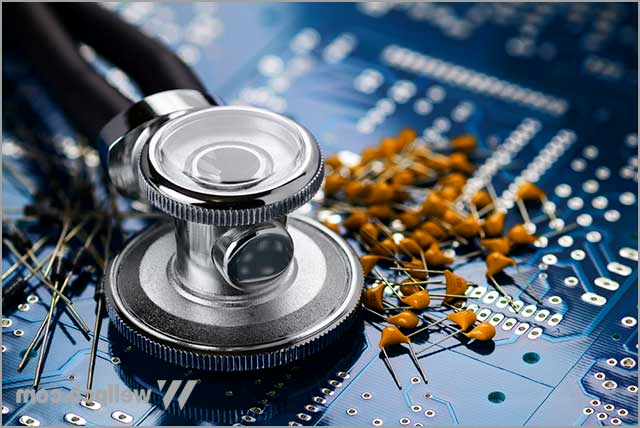
Used in the medical devices
Besides being beneficial in electronic equipment, they are also used in medical devices. They are beneficial in every sector of the medical industry and even in the diagnosis industry. Being in small size and lightweight in nature, they are the perfect option to use in the case of medical devices.
Industrial devices
Multi-facet PCBs in all actuality do demonstrate more strong than a few different choices at present available, settling on them a decent decision for applications where harsh taking care of might be an every day event. All things considered, multi-facet PCBs have become famous in a few modern applications, generally outstanding of which are modern controls.

Military and self-defense equipments
Leaned toward their sturdiness, usefulness and low weight, multi-facet PCBs are helpful in high velocity circuits, which is turning into an expanding need for military applications. They’re likewise preferred because of the guard business’ expanded development toward exceptionally conservative designing plans, as the little size of multi-facet PCBs passes on more space for different parts to thrive existing capacities.
Automotive equipment
Vehicles are depending on electronic parts increasingly more in the cutting edge time, particularly with the ascent of electric vehicles. Including GPS’s and installed PCs to front light switches and motor sensors constrained by hardware, utilizing the right sorts of parts turns out to be progressively fundamental in car plan. This’ the reason numerous carmakers begin to lean toward multi-facet PCBs over different other options. While they are little and sturdy, multi-facet PCBs are additionally exceptionally utilitarian and moderately heat-safe, making them a solid match for the inside climate of a vehicle.
What are the different types of PCBs?
We hope that you have understood what are PCBs, and now it is the time when you need to understand the different types of PCBs. There are many different types of PCBs, and it is the one that is made with varying types of materials. The PCBs are divided according to their layers and here, we have different types of them.
Single Layer PCB
As its name implies that single layer PCBs are the simplest form of PCB, and they are made with the most-easiest design. They are made with a single layer of PCB, which can be copper, and one side of this PCB is the non-conductive substrate.
Double Layer PCB
The double-layer PCB is made with one layer with the non-conductive substrate, and the other layer is made with a conductive material. These two conductive layers get attached along with each other with the help of the plated holes and having a substrate that is connected on both of the sides of the circuit boards.
Multi-layer PCB
As its name describes that the multilayer PCB is all made with the help of multiple layers. It has conductive layers, which are made on the top and even have it on its bottom. It is the board, which has the capability to get connected with around 40 layers. Its circuit with 40 layers is known as advanced Pcb.
High density interconnect or HDI PCB
The difference between the other types of PCB and high density interconnect is their design and structure. They are made to send or receive signals for around 1gigahertz. Depending upon the application, you can choose any type of HDI PCB. It is all used for advanced operations and has controlled impedance. The design of HDI PCB starts from the simplest to the complex one.