
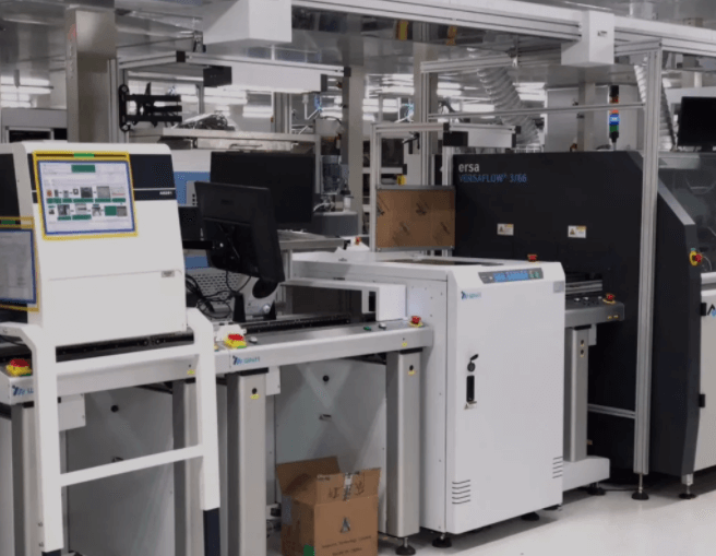
Introduction to wave soldering technology
DIP plug-in and SMD adhesive process special wave soldering is one of the important processes of modern electronic manufacturing in PCB assembly industry, although it has been affected by SMT technology, but there are still quite a lot of electronic components can not be completely replaced by SMT packaging technology, such as high reliability requirements of the plug and plug connectors, some high-power electrolytic capacitors. Therefore, wave soldering will also play an important role in the field of electronic manufacturing.
Wave soldering is a common automatic soldering technology in the electronic industry. It has the characteristics of reliable soldering quality, good appearance, good soldering consistency, easy operation, energy saving and reducing labor.
Technical requirements for high quality control of
wave solderingDIP wave soldering overview
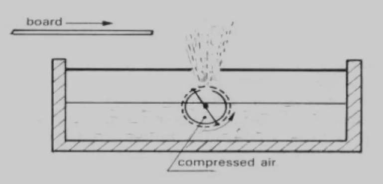
Wave soldering is a soldering process that the molten liquid solder, with the help of a pump, forms a specific soldering wave on the surface of the solder tank, and the PCB with the components is placed on the transmission chain, the soldering joint is realized by passing through at a specific angle and a certain immersion depth.
Wave soldering is used to make assembled printed circuit boards in a batch PCBA fabrication. It is called wave soldering because it uses wave-like soldering. Is mainly used for through-hole components and SMD components soldering of SMD adhesive (red glue) process, in the latter case, before through the molten solder furnace, through the SMT placement machine, the components and adhesive bonded on the surface of the printed circuit board (PCB).
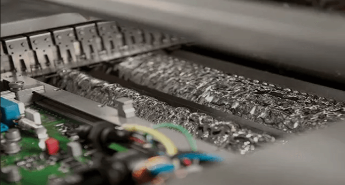
Wave soldering is to make the soldering surface of the plug-in PCBA circuit board directly contact with the high temperature liquid tin to achieve the purpose of soldering, the high temperature liquid tin to maintain a bevel, and by the special device to form a similar wave of liquid tin phenomenon, so called “wave soldering”.
Below is a schematic diagram showing the wave of molten solder paste passing through the bottom surface of the board, making the PCB pad and the component pins fully soldered and firmly connected.
Control requirements
The process of wave soldering, mainly can be divided into these several stages: install fixture, flux coating, preheating (temperature 90-100℃, length 1-1.2m), soldering and cooling.
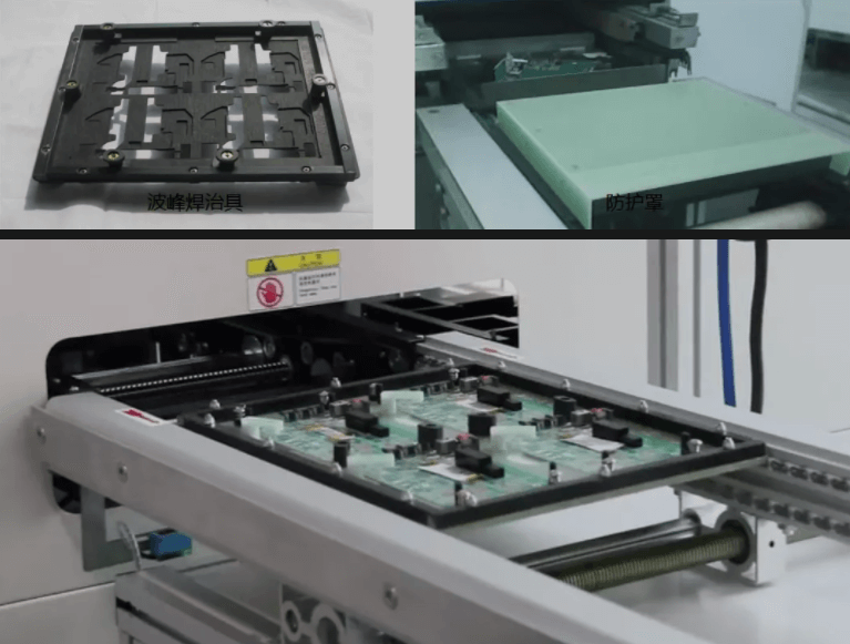
1. Install fixture:
Wave soldering requires high flatness of PCB board, and the thickness of PCB board of automotive electrical components is generally only 1.6mm, so the warpage requirement itself is very high. In the process of wave soldering, more attention should be paid to the degree of thermal deformation control. The clamping fixture installed on the PCB to be soldered can limit the degree of thermal deformation of the substrate and prevent the occurrence of soldering phenomenon, so as to ensure the stability of the soldering effect, which is particularly important for the thinner PCB.If the splashed tin residue is often left on the PCB during wave soldering, it can be considered to add a protective cover on the fixture. At same time, whether the fixture is cleaned regularly also needs attention.
2. Coating flux:
The function of flux is as follows:
● Clean the oxide that may exist on the surface of PCBA boards which waiting solderinrg;
● Prevent the re-oxidation of metal surface;
● Reduce the surface tension of liquid solder, improve the diffusion ability.
Now the general use of spray system for flux spraying, the process of the need to focus on control is the amount of coating and uniformity, that is, the requirement of uniform coating, and the amount of flux coating is moderate.Insufficient or uneven flux coating may result in insufficient activation of pads, resulting in missed and poor soldering.
The key points of control are as follows:
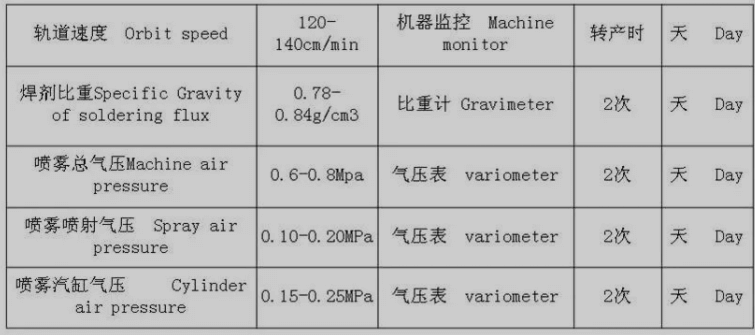
Some important monitoring parameters affecting flux coating include air pressure, flux specific gravity (concentration), transfer speed, etc. These parameters must be reflected in the first inspection.
For the uniformity of flux coating, fax paper can be pasted on the bottom side of the PCB. By comparing the area and density of flux spraying traces with standard drawings, visual inspection can be carried out. Using this method, the spray quantity can be quantified by weighing before and after spraying and calculating the weight change, which can be used as a reference for judging basis.
3. Preheating:
The functions of preheating mainly include:
Slow evaporation of flux
Insufficient preheating may cause the liquid solvent in the flux to vaporize violently when it reaches the peak of the wave, resulting in solder spatter and tin slag; Excessive preheating will cause the active ingredients of the flux to evaporate prematurely and lose the wetting effect, resulting in bridging or pointing during soldering.
Reduce the thermal stress produced during soldering
In the case of insufficient preheating, thermal stress caused by sudden heat during soldering may cause damage to some components.
As mentioned above, the critical control points for this process are preheating temperature and preheating time.
The general preheating temperature is 90~130℃, and the preheating time is 1~3min.The preheating process is well controlled, which is helpful to prevent the poor soldering, reduce the thermal impact of solder wave peak on the substrate, and effectively solve the warpage, delamination and deformation of PCB in the PCB soldering process.
4.Soldering:
Soldering Process:
(1)The PCB board in the entry area starts to contact with the wave peak at a certain Angle and depth.
(2)The heat transfer area is between the entry area and the separation area, and the circuit board is in direct contact with solder paste. Although parts contact with molten tin can reach the temperature of soldering paste instantly, but in order to better soldering, more time is needed.
(2)In the escape zone, the excess solder paste will be pulled back into the solder paste channel.
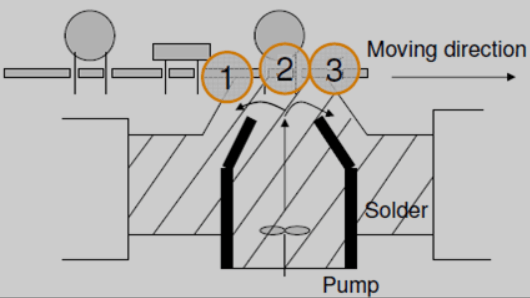
In the soldering process, there are many factors that affect the soldering quality. The parameters that need to be paid attention to include soldering temperature, transmission speed, orbit Angle, wave peak height and so on.
- Soldering temperatureWhen the welding temperature is too low, the expansion rate and wettability of solder will get worse, so that the solder pad or the components pins can not be fully wettable, resulting in defects such as poor soldering. When the soldering temperature is too high, it accelerates the oxidation of the pads, pins of the components, which is easy to generate false soldering.
- Transmission speedThe solder paste wave in abscission zone should be as smooth as possible, so the conveyor belt speed should not be too high.
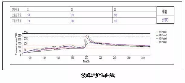
Normal parameters of wave soldering: furnace temperature 275℃, chain speed 1300 cm/min, relatively stable wave soldering furnace temperature curve (as shown in the figure below).
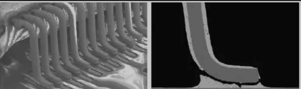
- Track AngleThe contact time between the PCB and the wave crest can be controlled by adjusting the Angle of the track, and the proper inclination helps to separate the liquid solder from the PCB faster. When the dip Angle is too small, the bridge is easy to appear. The dip Angle is too large, although it is conducive to the elimination of the bridge, but the solder paste too small, easy to generate false soldering. The orbital inclination should be controlled between 5° and 7°.
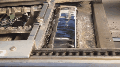
- Wave crest heightWave crest height refers to the solder paste height of PCB in wave soldering, which is usually controlled within 1/2~2/3 of the thickness of PCB board. Excessive crest height causes molten solder to flow onto the surface of the PCB, forming a “tin joint”. The height of the wave crest may change due to the passage of soldering working time, which should be properly corrected in the soldering process. The commonly used tools for measuring the height of the wave crest are depth gauge or high temperature glass.
The soldering process is a thermal processing process, a good soldering effect, need to consider solder formula, flux, components and PCB matching, design and process control parameters. There may be multiple reasons for a bad result. Next, we collected some practical and common bad wave soldering, analysis methods for the causes and suggestions for improvement.
Bridging
Bridges are adjacent solder pads that should not be joined together by solder paste. This connection is bound to cause an electrical failure.
The prevention of bridging should start from the source – design, so DFM analysis is particularly important. If the PTH components with pitch not less than 2mm is selected, the penetration of the soldering pins shall not exceed 2mm, the spacing of the copper rings shall not be less than 0.5mm, white solder mask shall be added between the copper rings.
If the pitch of the component is too small and the spacing between the copper rings is too small, it is recommended to cut the soldering pins out to 0.5mm, and add a tin-drag(titanium alloy, tinplate nickel plating) at the appropriate position in the tray to reduce the risk of bridging.
Low molten solder paste temperature, the fluidity of molten solder paste is poor, will cause bridging; Low preheating temperature, soldering temperature is insufficient, will also cause bridging.
The chain speed should be appropriate. Too low chain speed may accelerate flux consumption, resulting in decreased wetting of solder, resulting in bridging.
Replacement of a more active flux will help to reduce bridging because the active flux will increase wettability.
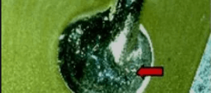
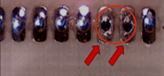
Cold Joints
Cold Joints is due to the lack of heat and other reasons for the solder joint appears poor wetting, gray and wrinkled.
Such defects are usually due to the lack of heat making the soldering time short, resulting in gray solder joints. Appropriately increasing the soldering time, adjusting the preheating temperature and solder melting temperature are helpful to improve the defect.If the solder joint seems broken and uneven, most of the reason is that the component is vibrating when the solder is about to cool to form the solder joint. In this case, pay attention to whether there is abnormal vibration of the pawls.Oxidation or contamination of the soldering surface can also lead to Cold Joints, which requires strict control over protection during storage and movement of incoming materials.
Such defects are usually due to the lack of heat making the soldering time short, resulting in gray solder joints. Appropriately increasing the soldering time, adjusting the preheating temperature and solder melting temperature are helpful to improve the defect.If the solder joint seems broken and uneven, most of the reason is that the component is vibrating when the solder is about to cool to form the solder joint. In this case, pay attention to whether there is abnormal vibration of the pawls.Oxidation or contamination of the soldering surface can also lead to Cold Joints, which requires strict control over protection during storage and movement of incoming materials.
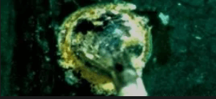
Flux residue
Flux residue occurs when flux is not completely removed from the solder. Corrosion of flux will affect solder joint reliability.
The flux residue can be reduced by reducing the flux spraying amount or increasing the preheating temperature appropriately and increasing the flux consumption.
The rosin resin solid content in the flux is too much or the quality is not good, it is easy to cause too much residual, to replace the flux according to the product.
Increasing soldering time to increase flux consumption can also reduce flux residue.
The flux residue can be reduced by reducing the flux spraying amount or increasing the preheating temperature appropriately and increasing the flux consumption.
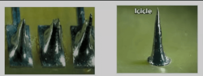
Lcicles
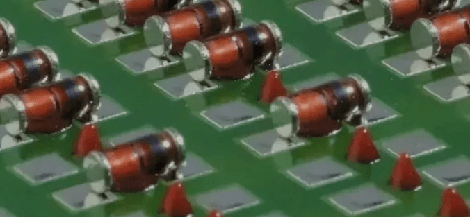
Lcicle is an abnormal conical or nailed joint. The main reason for pulling the point is that the solder does not contract when it is cooled. Such solder joints may be too close to the adjacent plate during system assembly to violate minimum electrical clearance requirements or short circuit.
Lcicle has a great direct relationship with the temperature, preheating temperature is low, low solder melting temperature will make after the peak due to insufficient temperature, solder paste melting can not effectively shrink. The low melting temperature increases the viscosity of the molten solder and intensifies the formation of lcicle. It is recommended to reset the measured temperature curve.
Flux also has a lot to do with Lcicle. When the flux activity is not enough or the concentration decreases, the flux is not competent to deoxidize and reduce the surface tension, so that the molten solder can not effectively shrink when leaving the tin furnace. Increasing flux concentration, activity and spraying amount, increasing flux spraying pressure and improving its penetration are all helpful to the elimination of Lcicle.When the chain speeds too fast, excess solder may not be pulled back to the solder stove, causing Lcicle.Individual due to the length of the solder pins caused by the lcicle, the solder pins should be cut short. It is recommended that the penetration (L) of the solder pins should not be greater than 2mm.
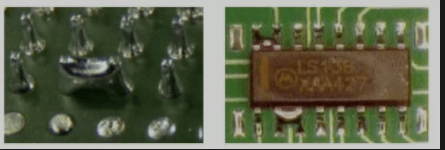
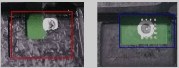
The pin of the QFP is peeled
QFP pin peeling due to insufficient solderingDecreated joint strength due to insufficient solderingDuring wave soldering, the reflow soldering section will melt again, and the warpage of the substrate during soldering and the pressure during assembly will cause the joint to peel offPrint the right amount of solder (stencil thickness, opening area)Adjust the design area of solder pads (to ensure full solder joints are formed)
Missing soldering
The solder paste does not wet the solder pins and pads and does not form an effective solder joint connection.
When the length of the solder pin is less than the thickness of PCB board, poor and missing soldering are most likely to occur. Therefore, to do a good job of DFM, select components with soldering pins that can penetrate through the soldering surface at least (L) 0.5mm. When there is no gap between the bottom surface of the through-hole components and the PCB surface, the gas evaporated by the flux at high temperature has no channel to escape, and it remains in the hole and prevents the solder from wetting the hole wall. Therefore, select components must select components with gaps.Oxidation and contamination of soldering pins and through-holes will reduce their solderability and eventually lead to missing soldering. So, protecting incoming material is an important measure to ensure soldering quality.The shading effect of the crest trays can also cause missing soldering. In this case, thinning the tray, increasing the opening of the tray (the space between the soldering pad and the outer wall of the tray should not be less than 2.5mm), and using thinner titanium alloy materials can improve the missing soldering.
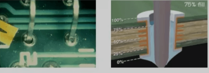
Solder paste is not fully filled of PTH components
Insufficient solder paste filling in the through hole refers to that the solder filling height in the hole does not meet the IPC requirements (50% or 75% of PCB thickness), or does not meet the customer requirements, which affects the reliability of soldering.
If the defect always occurs on the same component, the reason may be that the tray design has a shading effect (too little space between the outer wall of the fixture and the soldered surface), which reduces the contact area between the molten solder paste and the surface to be soldered. The improvement measures at this point are to partially thin the pallet (synthetic stone material with a minimum thickness of 0.5mm) or to use a thinner titanium alloy (with a minimum thickness of 0.2mm).
Oxidation and pollution on the soldering surface will also lead to insufficient solder paste not enough for soldering. At this time, elemental analysis should be carried out on the component pin or the surface of the hole wall to find out the pollutants and pollution sources. Of course, choose a more active flux will ameliorate the problem.
The hole size does not match, and the connection between the through hole and large grounded copper foil will also lead to insufficient filling, especially for large electrolytic capacitors. This situation needs to be improved by DFM design in advance.
Temperature is also a factor. When the preheating is insufficient, the flux activity decreases; Insufficient soldering temperature will cause the insufficient filling, this requires raising the temperature and resetting the soldering temperature curve.
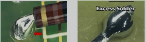
Excess Solder
The characteristic of excess solder is that the solder will completely wrap the soldering pin, and the wetting Angle is greater than 90 degrees.
If the excess solder is the whole batch, the first check is the temperature factor. Preheating temperature is too low will make the high viscosity of excess solder. It is suggested to re-optimize the soldering temperature curve.
The copper content in the solder furnace is too high will also make the tin in the tin furnace molten viscosity increased, resulting in excess solder. It is suggested that the copper content of molten solder paste should be checked regularly to ensure that the copper content is within a controllable range.
If the equipment parameters are normal, the solderability of PCB should be considered. Due to excessive oxidation and pollution of the pads and holes, the solderability is very poor, which results in that the excess solder cannot fully wetting the soldering surface and can only form a wrapping. In this case, it is suggested to analyze the solderability of PCB. If necessary, SEM and EDX testing can be added to urge the board manufacturer to improve the manufacturing process to improve the quality of PCB board and transport protection.
Reduced flux activity may also cause this defect, because the flux with low activity can no longer play its function. It is recommended to replace the flux at this time.
Influence of PCB quality on wave soldering
- There is green solder mask in the component hole, which leads to poor solder plating in the hole. Need to insert the PTH components, the hole is not allowed to have annular solder mask, so the green solder mask in the PCB component holes should not exceed 10% of the hole wall, and the number of holes which has green solder mask should not exceed 5%.
- Insufficient copper plated leads to poor tin plating in the hole.
- Insufficient thickness of copper, tin, gold, etc. In general, the hole wall thickness should be greater than 18μm.
- The hole wall is too rough, resulting in poor tin plating or poor soldering in the hole. If the roughness of the hole wall is too large, some areas will affect the effect of tin application.
- The holes are moist, leading to poor soldering. PCB packages that are not dried or cooled after drying, and left for a long time after unpacking, etc., will cause moisture in the holes, resulting in poor soldering or bubbles.
- The size of the pad is too small, resulting in poor soldering. Disconnection or gaps in hole pads may result in poor soldering. In general, the size of the pads should be greater than 4mil.
- The inside of the hole is dirty, resulting in poor soldering.inadequate cleaning of PCB, such as unpickled gold plate, leads to impurity and dirt residue on holes and pads, affecting soldering.
- Because the hole size is too small, the parts cannot be inserted into the hole, resulting in failure of soldering.
- Due to the offset of the positioning hole, the parts cannot be inserted into the hole, leading to the failure of soldering.
Failure analysis of SMD adhesive through wave soldering
In the production of PCB assembly process, many electronics factories will use SMD adhesive (red glue) process to make SMT assembly process. In this process will encounter a variety of components fall off the problem, especially the SMD adhesive process in the wave soldering (especially diode) often encounter the fall off problem.
A detailed solution for the reasons and solutions of the parts falling off during the wave soldering of SMD adhesive process. The content is as follows:
- If the component falls off together with the solder mask of PCB, we will judge it’s PCB problem (the adhesion of solder mask is not enough).
- Check the PCB to see whether there is scratch at the place where the components fall off. The scratch place where the component falls off will also make the adhesion of the solder mask insufficient, which can produce the drop of component after the PCB passes reflow process.
- Check the PCB to see whether the components drop regularly. If it is fixed to drop a few components, you have to consider whether the hole of the SMD adhesive stencil is blocked, and the amount of SMD adhesive s too little.
- If the components drop off, and the SMD adhesive was still stuck on it. We can judge that there was a problem with the incoming material of the components or PCB (such as surface treatment problem of PCB or components oxidation.
Technical requirements for high quality of wave soldering
The refinement development of electronic products leads to the increasing complexity of PCBA assembly, large differences between the various component packages on the PCB board and smaller assembly gaps between the components have contributed to the wide application of selective wave soldering.
Selective wave soldering can complete some PCBA wave soldering with complex structure, such as:
More and more PTH components are available with small pitch, such as 0.5mm pitch and smaller.
The solder pads of PTH component is too close to the SMD component to satisfy the traditional design of wave soldering fixture.
Double – sided plug-in components, the height of the plug-in components can not meet the traditional wave soldering.
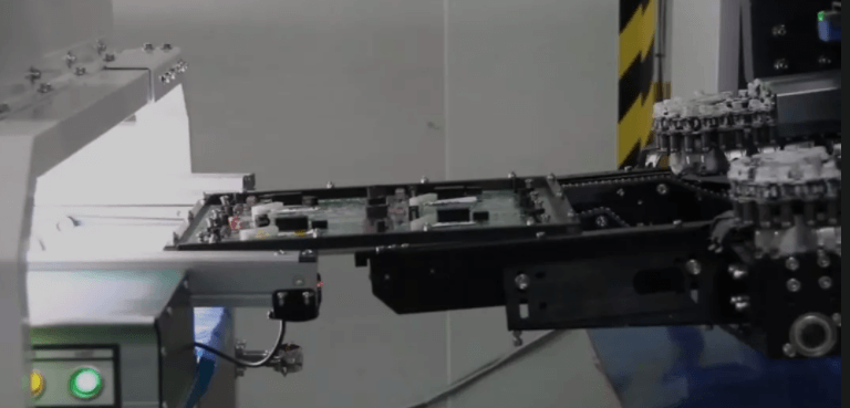
DIP selective wave soldering
DIP selective wave soldering
Compared with the traditional wave soldering process, the selective wave soldering process reduces the flux consumption, reduces the solder splash and the processing cost because of the single point of rosin spraying.
The most obvious difference between selective wave soldering and traditional wave soldering is that in traditional wave soldering the lower part of the PCB is completely immersed in the liquid solder, whereas in selective wave soldering only a certain area is in contact with the solder paste. In the soldering process, the position of the solder is fixed, and the manipulator drives the PCB to move in all directions. Flux must also be applied before soldering.
In contrast to wave soldering, flux is only applied to the bottom side of the PCB to be soldered, not the entire PCB, selective wave soldering is performed by applying flux, then preheating the circuit board/activated flux, and then using a soldering nozzle. The traditional soldering of artificial soldering iron requires point-to-point soldering for each point of the circuit board, so there are more soldering operators.
Selecting wave soldering is a production line type of industrial batch production mode. Different sizes of soldering nozzles can be used for batch soldering. Usually, the soldering efficiency can be improved dozens of times more than manual soldering (depending on the design of the specific circuit board).