
How to make a good PCB board
Everyone knows to do the schematic diagram of the PCB is designed into a real PCB, please don’t underestimate this process, there are a lot of things on the principle of practicable in engineering that has difficult to achieve, or some PCB manufacturers can realize and others not achieve them, so it is not difficult to make a PCB, but make a good PCB board is not an easy thing. The two major difficulties in the field of microelectronics are the processing of high frequency signals and weak signals. In this respect, the level of PCB production is particularly important. The same schematic design, the same components, different PCB factories make PCB have different results, so how to make a good PCB board?
1.Make clear of the design goal
Received a design task, must clear the design goals first, is a common PCB board, high-frequency PCB, small signal PCB or there are both high frequency and small signal of the PCB, if it is a common PCB, as long as do reasonable layout and tidy, mechanical size accurate, that’s will be fine.
When there are more than 40MHz signal lines on the board, special considerations should be taken into account for these signal lines. If the frequency is higher, there will be more stringent restrictions on the length of the trace. According to the distributed parameter network theory, the interaction between the high-speed circuit and its traces is the decisive factor, which cannot be ignored in the system design. With the increase of the transmission speed, the opposition on the signal line will increase correspondingly, and the crosstalk between adjacent signal lines will increase in direct proportion. Generally, the power consumption and heat dissipation of high-speed circuits are also very large, so enough attention should be paid when making high-speed PCB.
When there are millivolt or even microvolt weak signals on the board, these signal lines need special attention. Small signals are too weak to be easily interfered with by other strong signals. Shielding measures are often necessary, otherwise, the signal-to-noise ratio will be greatly reduced. So that the useful signal is drowned out by the noise and cannot be extracted effectively.
The debugging of the board should also be considered in the design stage, the physical location of the test point, the isolation of the test point, and other factors can not be ignored, because some small signals and high frequency signals can not be directly added to the probe to measure.
In addition, some other related factors should be considered, such as the number of layers of the board, the packaging of the components used, and the mechanical strength of the board.Before making a PCB board, you should have a clear idea of the design goals of the design.
2.Understand the PCB layout and PCB routing requirements of the components used
As we know, some special components have special requirements for layout and routing, such as the analog amplifiers used in LOTI and APH, which require a smooth, low-ripple power supply. The analog small signal part should be placed as far away from the power device as possible. On the OTI board, the small signal amplification part is specially equipped with a shielding cover to shield the stray electromagnetic interference. The Glink chip used on the NTOI board adopts the ECL process, which consumes a lot of power and generates a lot of heat. Therefore, special consideration must be given to the heat dissipation problem in the layout. If natural heat dissipation is adopted, the Glink chip should be placed in a place where the air circulation is relatively smooth, and the heat emitted can not exert a great influence on other chips. If the board is equipped with loudspeakers or other high-power devices, it may cause serious pollution to the power supply, which should also be paid enough attention to.
3.Component placement considerations
One of the first factors to be considered in the PCB design of components is electrical performance.The actual size (occupied area and height) of components and the relative position between components must be considered to ensure the electrical performance of the circuit board and the feasibility and convenience of production and installation. Put the closely connected components together as much as possible, especially for some high-speed lines, and make it as short as possible. Separate the power signal from the small signal components. In the premise of meeting the circuit performance, but also consider the components placed neatly, beautiful, easy to test, the mechanical size of the board, socket location and so on also need to be seriously considered.
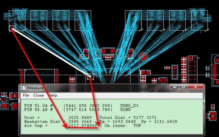
The transmission delay time of grounding and interconnection in high-speed systems is also the first factor to be considered in system design.The transmission time on the signal line has a great impact on the overall system speed, especially for high-speed ECL circuits. Although the speed of the integrated circuit block itself is very high, the increase of delay time due to the use of ordinary interconnects on the board (about 2ns delay for every 30cm line length) can greatly reduce the system speed.
4.PCB routing
PCB routing is the most important procedure in the whole PCB design. This will directly affect the performance of PCB board. In the design process of PCB, the routing is mainly carried out according to the following principles:
(1)In general, the power lines and ground lines should be first designed, in order to ensure the electrical performance of the circuit board. To the extent possible, try to widen the width of the power supply, ground line, it is best to be wider than the power line, their relationship is ground line> power line > signal line, usually, the width of the signal line is: 0.2 ~ 0.3mm, the minimum width of up to 0.05 ~ 0.07mm, power line is generally 1.2 ~ 2.5mm.PCB for digital circuits can be used with wide ground conductors to form a circuit, that is, to form a ground grid (the ground for analog circuits cannot be used in this way)
(2)High frequency lines should be placed advanced, the input and the output of the edge line should avoid adjacent parallel, so as not to produce reflection interference.
(3)Any signal line should not form a loop, if unavoidable, the loop should be as small as possible; through-hole of the signal line should as few as possible;(4)Keep the key lines short and thick, and add protection on both sides.
(5)When transmitting sensitive signal and noise field band signal through flat cable, the way of “ground – signal – ground” should be used.
(6)Test points should be reserved for key signals to facilitate production and maintenance testing.
(7)After the routing of the schematic is completed, the routing should be optimized; At the same time, after the preliminary network inspection and DRC inspection is correct, the un-routing area is filled with a ground line, and a large area of copper is used as a ground line. On the printed circuit board, the places that are not used are connected with the ground as a ground line. Or made to be multilayer board, power supply, ground line place on a separate layer.
PCB routing requirement
1.Track
In general, the signal line width is 0.3mm(12mil), the power line width is 0.77mm(30mil) or 1.27mm(50mil); The space between tracks, between tracks and pads, is larger than or equal to 0.33mm(13mil). In practical application, the space should be considered when conditions permit; When the track density is high, it may be considered (but not recommended) to use two tracks between IC pins, the width of which is 0.254mm(10mil), and the spacing of which is not less than 0.254mm(10mil). Under special circumstances, when the device pins are dense and the width is narrow, the line width and line spacing can be appropriately reduced.
2.Pad
The basic requirements for pad and via are: the diameter of the pad should be greater than 0.6mm than that of the via; For example, universal pin-type resistors, capacitors, and integrated circuits, etc., using pad/via the size of 1.6mm/0.8mm (63mil/32mil), socket, pin and diode 1N4007, etc., using 1.8mm/1.0mm (71mil/39mil). In practical application, it should be determined according to the size of the actual components. If conditions permit, the size of the pads can be appropriately increased. The mounting holes of the designed component on PCB board should be about 0.2 ~ 0.4mm larger than the actual size of the component pin.
3.Via
Normally 1.27mm/0.7mm(50mil/28mil); When the line density is high, the size of the via can be reduced appropriately, but should not be too small. 1.0mm/0.6mm(40mil/24mil) can be considered.
4. Spacing requirements for pads, tracks and vias
pad and via: ≥ 0.3mm(12mil)pad and pad: ≥ 0.3mm(12mil)pad and track: ≥ 0.3mm(12mil)track and track : ≥ 0.3mm(12mil)When the high density of tracks:pad and via : ≥ 0.254mm(10mil)pad and pad : ≥ 0.254mm(10mil)pad and track: ≥ 0.254mm(10mil)track and track : ≥ 0.254mm(10mil)
5.Netcheck, DRC check and structure check
Firstly, on the premise that the PCB design of the circuit schematic diagram is correct, net check the physical connection relationship between the generated PCB network file and the schematic network file, and modify the design in time according to the output file to ensure the correctness of the routing connection relationship.
After the network check is passed correctly, conduct the DRC check on the PCB design, and modify the design according to the output file in time to ensure the electrical performance of the PCB routing.Finally, the mechanical installation structure of PCB should further check and confirm.
Three spcial routing skills in PCB lAYOUT
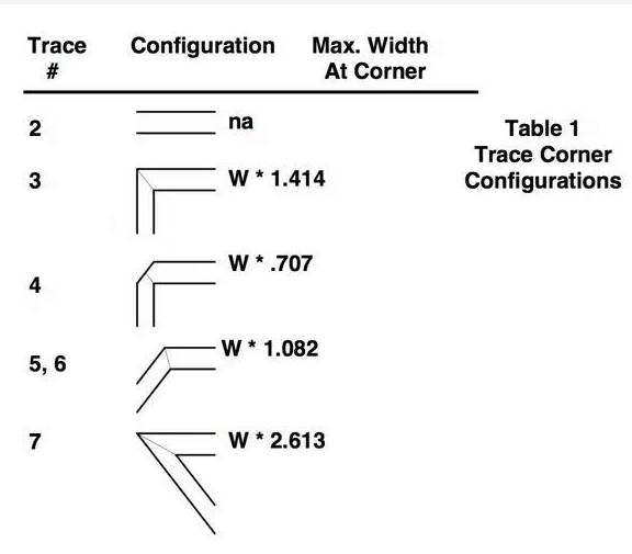
1.Right Angle routing
The influence of right-angle routing on the signal is mainly reflected in three aspects: first, the corner can be equivalent to the capacitive load on the transmission line, which slows down the rise time;Second, impedance discontinuity will cause the reflection of the signal; The third is the EMI generated by the right-angle. To the RF design field above 10GHz, these small right angles may become the key object of high-speed problems.
2.Differential routing
Differential Signal is when the driver sends two equivalent, inverted signals, and the receiver compares the difference between the two voltages to determine whether the logical state is “0” or “1”.The pair of lines that carry the differential signal is called the differential lines.Compared to ordinary single-ended signal routing, the most obvious advantages of differential signals reflect in the following three aspects: 1), high interference immunity due to the very good coupling between the two differential lines when external noise interference is present. It can couple to both lines at the same time, while the receiving end only cares about the difference between the two signals. So can completely cancel out the common external noise. In the same way, because the polarity of the two signals is opposite, the electromagnetic field radiated by them can cancel each other. The closer coupling, the less electromagnetic energy is released to the outside.3), Accurate timing positioning. Because the switch change of the differential signal is located at the intersection of two signals, unlike the ordinary single-ended signal, which depends on the high and low threshold voltage to judge, it is less affected by the process and temperature and can reduce the error in the timing. LVDS (Low Voltage Differential Signaling), which is popular at present, refers to this small amplitude differential signaling technology.
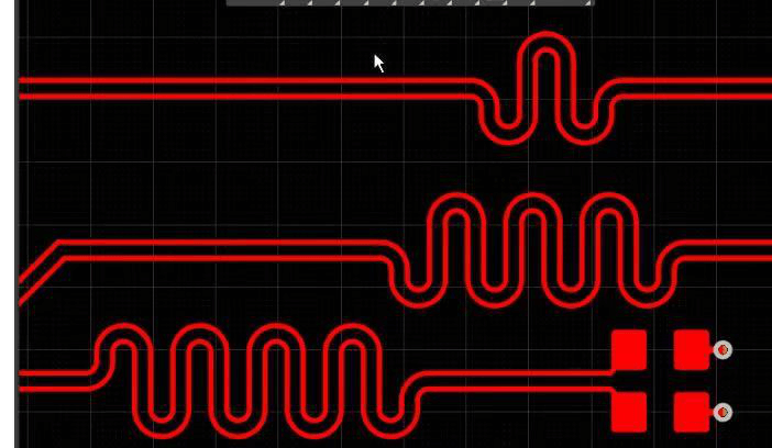
3.Curved routing
Curved routing is a kind of routing method often used in PCB Layout. Its main purpose is to adjust the delay, to meet the timing design requirements of the system. The two most critical parameters are parallel coupling length (Lp) and coupling space (S). Obviously, when the signal is transmitted on the curved routing, the coupling between parallel line segments will occur in the form of differential mode. The smaller S is, the larger Lp is, and the greater the coupling degree is. This may lead to a reduction in transmission delay and a significant reduction in signal quality due to cross, the mechanism of which can be referred to the analysis of common mode and differential mode cross.
Some possible PCB layout problems, causes, and the effects
| Problem | Cause | Effect |
| LNA/tank circuit arrangement (receiver) | Inductor orientation | RF feedthrough |
| Degeneration/π-network arrangement (transmitter) | Inductor orientation | RF feedthrough |
| Shared ground vias between legs of π network | Via parasitics | Feedthrough, RF leakage |
| Shared ground vias between receiver blocks | Via parasitics | Crosstalk, RF feedthrough, RF leakage |
| Long traces for decoupling capacitors | Higher-impedance connections | Reduced decoupling |
| Wide component placement | Increased parasitics, ground loops | Detuning, crosstalk, feedthrough |
| Colinear traces in the transmitter circuit | Filter bypassing, i.e., power amplifier (PA) directly to antenna | Harmonics radiation |
| Top-layer copper pours | Parasitic coupling | RF leakage, RF interference |
| Discontinuous ground plane | Return current concentration | Crosstalk, feedthrough |
| Crystal connection trace length | Excess capacitance | LO frequency pulling |
| Crystal connection trace separation | Excess capacitance | LO frequency pulling |
| Ground plane under crystal pads | Excess capacitance | LO frequency pulling |
| Planar PCB trace inductors | Poor inductance control |