
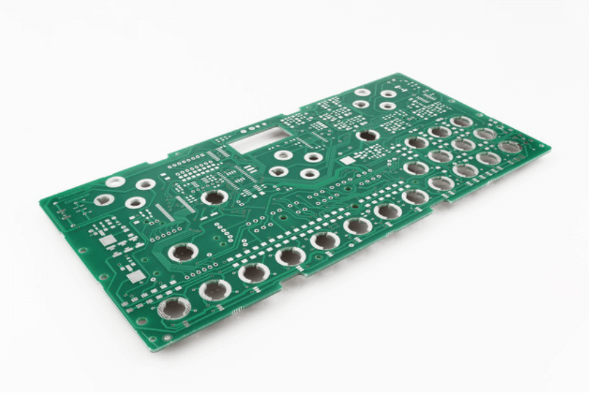
What is Light PCB Assembly?
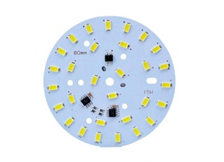
The technology of printed circuit boards is a useful tool in supporting LEDs. These sheets are made of fiberglass, metal, or other materials. And can connect electronic components. These boards are often referred to as LED lighting pcb assemblies and are critical to many LED applications.
Advantages of light pcb assembly
Low thermal emissions
This is by far one of the most important reasons for using China led pcb assembly.
The most conventional light sources or other light sources in the circuit have always had problems with heat dissipation. However, in the case of light pcb assembly , this is not a big problem. Many emerging technologies are combined with heat sinks that eliminate even a very small amount of heat. This in turn allows the entire circuit and other components to operate at relatively very low temperatures.
Low power consumption
Light pcb assembly also have a significant advantage in that they consume very little power. Because of this, LED bulbs are starting to become the new energy-efficient lights and are being widely promoted everywhere. In general, when one uses LEDs, the demand for electricity is reduced by as much as ten times compared to other lighting sources.
Lightweight construction
Light pcb assembly are lighter than traditional circuitry and designs.
Ease of manufacturing and integration
Manufacturing of technology is never an easy task. With a large number of components, arrays, etc., there is a lot of work going on in the background before your average technology reaches the end user. LED PCBs are fairly simple and easy to manufacture, while saving manufacturers money.
Light pcb assembly is largely dust and moisture resistant
While this in itself is not absolute, it is more durable and long-lasting than more traditional forms of circuitry and light sources. More specifically, they are ideal for outdoor use, where they are almost constantly exposed to dust and moisture.
Additionally, the structure can be made stronger by adding safety features and sealing systems to it.
Applications of Light PCB Assembly
Telecommunications

Transportation
Light pcb assembly can use in the transportation and aviation industries, as well as traffic lighting. There are also signal lights, highway tunnel lighting, and street lighting. LED PCS is used to indicate and provide interior lighting in airports and other aviation industries.
We can use an aluminum LED pcb assembly machine for automotive accessories such as indicators, brake lights, headlights, and other applications. Aluminum led pcb assembly machines would be suitable for the automotive industry because they offer characteristics such as durability and economy.

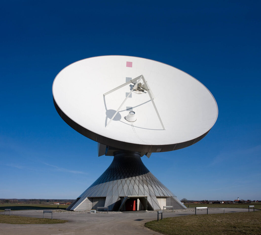
Computer and military
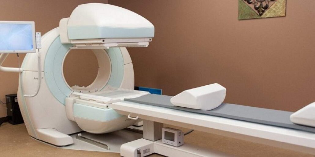
Medical
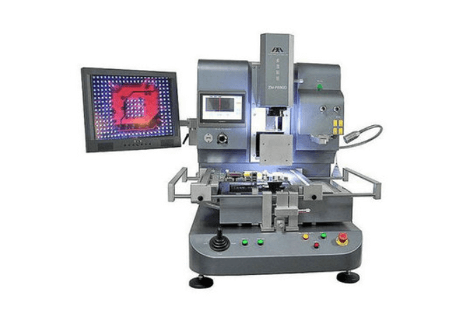
How to remove smd led from pcb
Problems and solutions encountered in light PCB assembly
Control current in light PCB assembly
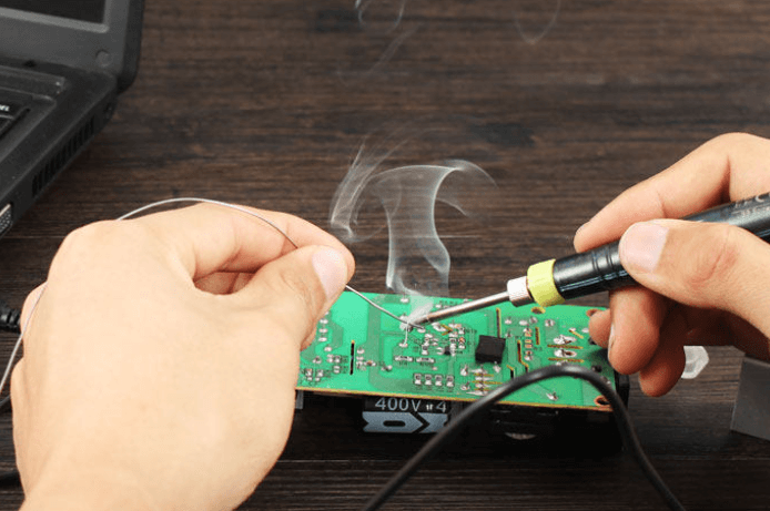
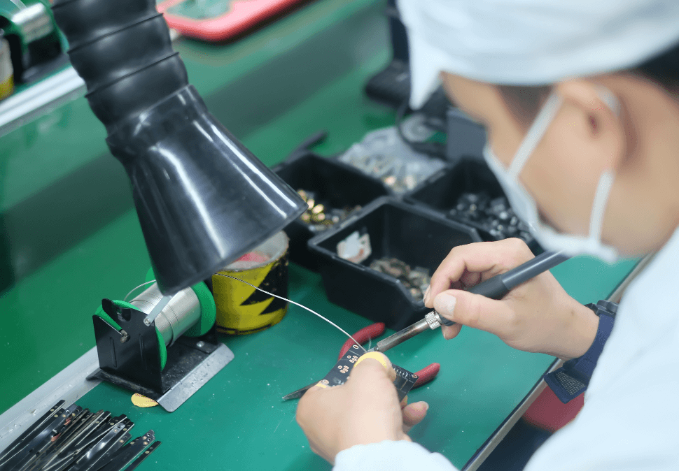
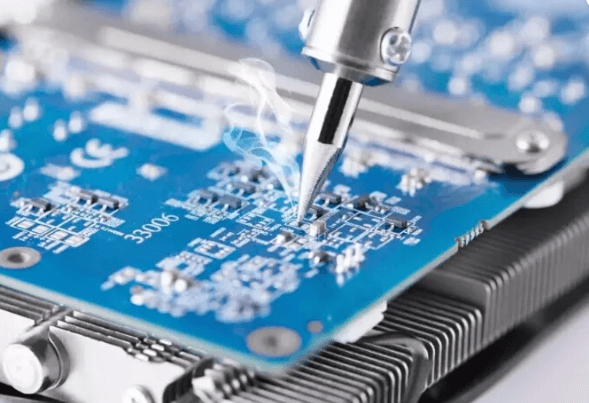
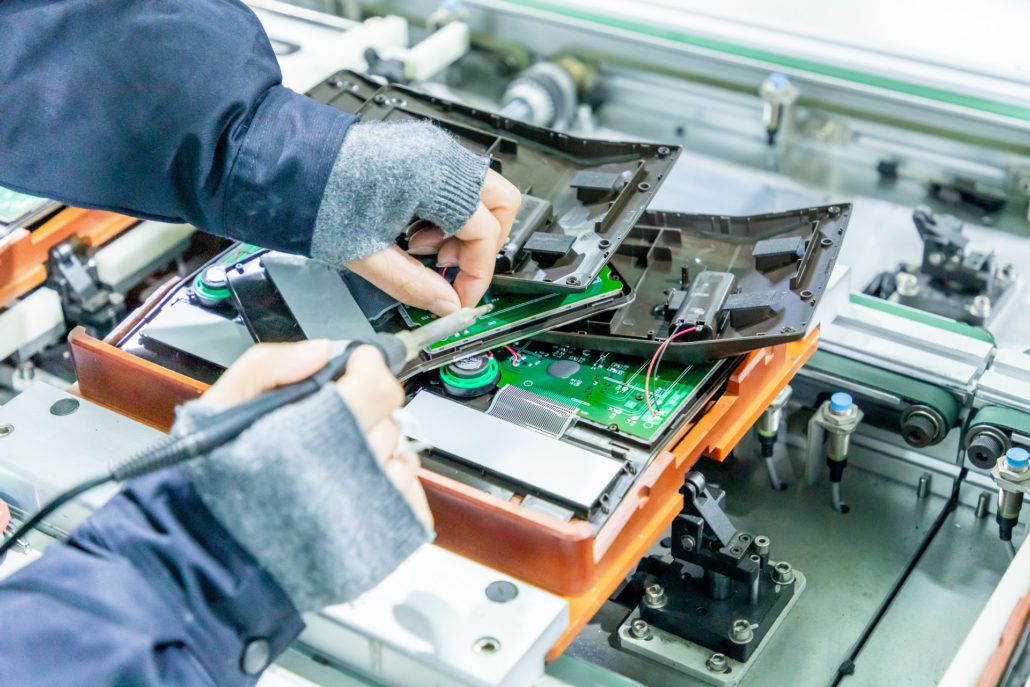
Solder LED components in pcb led lighting assembly
- Solder bridges: When you make an accidental connection while soldering, it may lead to a short circuit.
- Soldering may also occur when the component is warping.
- You want to make sure that your solder head is clean and tidy so you can create a good joint. This will allow you to use enough heat induction when soldering.
- Begin by soldering the smaller parts, then moving on to the larger components. It allows you to quickly assemble the PCB.
Light pcb assembly material selection
LED PCB assembly with aluminum substrates
1. Aluminum substrate increases the stability of the PCB. Just because the heat transfer is better than other materials, it will not affect other parts.
2. Aluminum is strong and durable and can withstand high temperatures.
3. In addition to being durable, aluminum is lightweight and more comfortable to handle and even transport.
4. Compared to many other panels, aluminum is cheaper. It is also recyclable and therefore environmentally friendly.
5. Aluminum has better heat transfer capability and therefore can work at low temperatures, thus ensuring a longer working time. Aluminum will extend the life of the PCB.
6. When using aluminum, heat moves faster. Thus, it functions more efficiently and does not exceed the temperature specified for it.
Embedded pcb led lighting assembly
In small and thin electronic products for custom LED PCB assembly, this is the most suitable for the use of embedded LED PCB. The pcb led lighting assembly is suitable for medical equipment, low-light environment, as well as some aviation and marine equipment. The following are some of the benefits of using embedded pcb led lighting assembly.
1. Light pcb assembly are dust and even moisture resistant
2. They are lightweight and less noticeable
3. LED pcb assembly is available in a choice of colors, sizes, and light intensities
4. Light pcb assembly has a lower backlight coating and membrane switches
5. They consume less power and are therefore very energy efficient
6. PCB led lighting assembly works better on silver and copper flexible membrane switches.
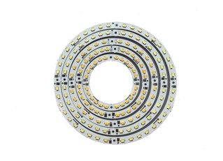
Single point, surface mount and integrated LED
These are lighting pcb assembly that are designed by the manufacturer so they can meet the user’s specifications. They are available in a variety of sizes and colors. These LEDs can be placed in any area. They can also create colors and reduce the size of the produced light. Each one of these lights has its advantages and disadvantages.
Advantages
1. Light source optimization
2. Fixture has added value
3. much easier to make new designs when dealing with integrated LEDs
Disadvantages
1. They have an expiration date
2. They can be difficult to replace
3. Most of them do not have solid warranty coverage
Light PCB Assembly Specifications
1. Number of layers
These layers consist of aluminum and magnesium.
2. Types of layers
Usually, the base layer is made of aluminum alloy metal. Aluminum alloy substrates used to make the base are ideal for through-hole technology for transfer and heat dissipation. The thermal barrier is made using some ceramic polymers with good viscoelastic properties.
3. The number of flexible PCBs
4. Size
5. Substrate
6. Minimum spacing
7. Hole size
8. Solder mask
9. Silkscreen
10. Connectors
11. Ribs
12. LED PCB assembly surface treatment
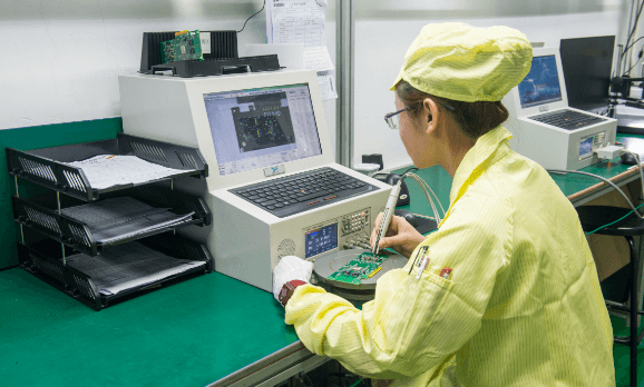
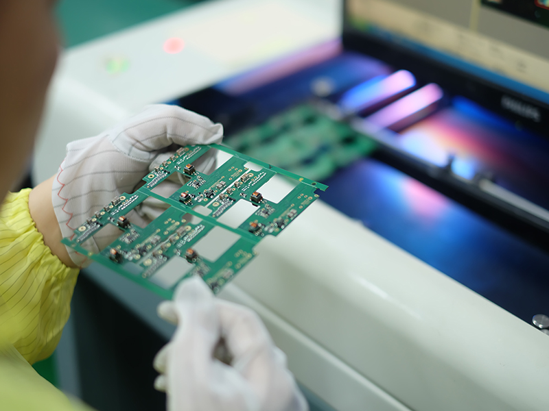
Light PCB Assembly Process
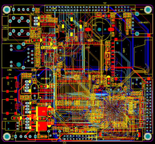
Step 1: Design and Output
Step 2: From movie to file
After the PCB designer has exported the PCB schematic file, and the manufacturer has done a DFM inspection, PCB printing can begin. To print the board, the manufacturer uses a special printer known as a plotter. This makes photo films of the printed PCB. All films should have holes punched to ensure perfect alignment. Adjusting the table where the film is placed determines the accuracy of the holes. When the table is in the right alignment, holes are punched. These holes do use to position the pins in the next stage of the imaging process.
Step 3: Print the inner layer
The previous step of the film creation did aim at drawing out the graphics of the copper path. Now it’s time to print the graphics from the film onto the copper foil. In PCB construction, cleanliness is really important. The copper-faced laminate is cleaned and put into a purged environment. At this stage, it is crucial that no dust particles are deposited on the laminate. Otherwise, errant dirt specks may cause circuits to short or remain open.
Steps 4: Remove unwanted copper
Step 5: Layer alignment & optical inspection
Once all layers are cleaned up and ready to go you will need to align them all. Alignment holes align the inner layers with the outer layers. The technician places these layers into a machine called an optical punch, which allows for precise correspondence to accurately punch the alignment holes.
Step 6: Layering and gluing

Step 7: Drilling
To find the location of the drill target, the X-ray locator identifies the correct drill target point. The appropriate alignment holes are then drilled to hold the stack for a series of more specific holes. Once the drilling is complete, additional copper lines at the edge of the production panel are removed with a contouring tool.
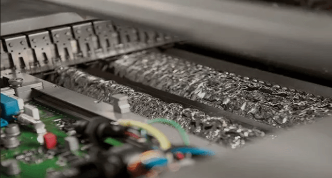
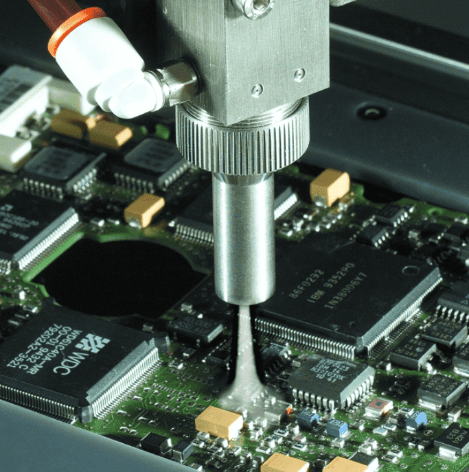
Step 8: Copper Deposition and Plating
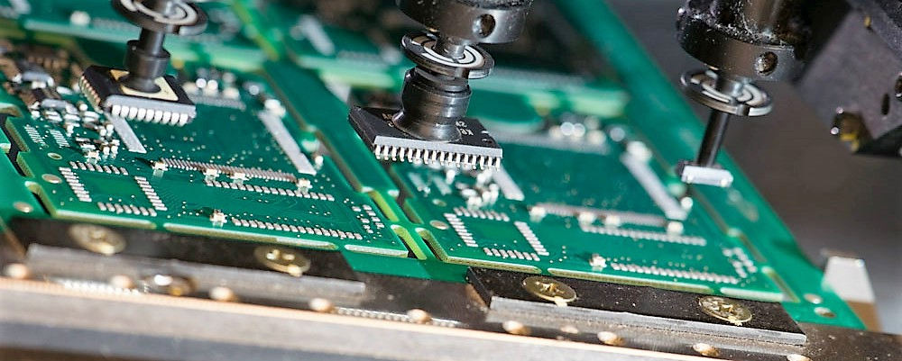
Step 9: Outer layer imaging
Step 3: We apply the photoresist on the panel. This step is similar to the previous one except that we now image the outer panel with the PCB design. To prevent contaminants adhering to the surface of the layer, we first place the panel in a sterile chamber. Next, we apply a layer with photoresist.
This is the reverse of the inner layer. Next, the outer plate must be examined to ensure that there is no photoresist.

Step 10: Plating
Step 11: Final Etching
Step 12: Apply Solder Resistant
The panel must clean before the solder resist is applied to both sides. The UV light will direct at the board through the solder resist photographic film. The remaining covered area will not harden and will remove. The board is then placed in the oven to cure any solder resist.
Step 13: Surface treatment
We chemically plat the PCBs with silver or gold to increase solderability. Some PCBs are also subject to hot-air leveling. Hot air leveling results in uniform pads. Achieving light pcb surface finish by LED PCB assembly process. UETPCB can apply a variety of surface finishes to meet customer requirements.
Step 14: Silkscreen
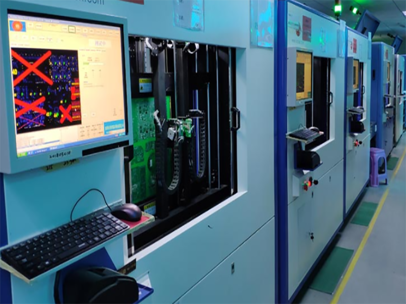
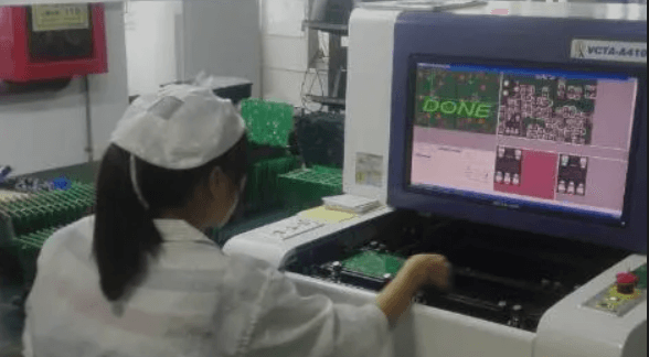
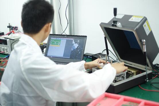
Step 15: Electric Testing
Step 16: Analysis and Scoring
Packaging LED PCB after Assembly. Types of Light PCB assembly packaging:
- Lamp-LED
- Surface Mount Device-LED
- Side-LED
- Top-LED
- High power-LED
- Flip chip-LED