
As a PCB and PCB assembly manufacturer, we must let you know what our PCB assembly services are. PCB assembly is a complex and lengthy process involving many different stages. Prototype pcb assembly is also critical for achieving the final product’s functionality. Each step must be executed accurately by paying maximum attention. Any small mistake in the PCB assembly process can lead to the failure of the final assembly. To help you further understand the entire PCBA process, we have explained the pcb assembly steps in detail below.
Before the Assembly Process
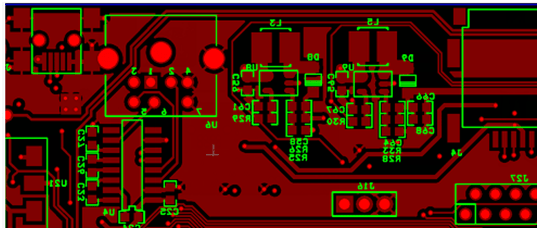
Design for Manufacturability (DFM) Check
Then what’s the DFM CHECK? before the actual assembly process, manufacturers thoroughly check the PCB design file to check the functionality and manufacturability. This stage, we called DFM, checks design specifications of a PCB, analyze any missing, redundant or potentially problematic features. The stage helps detect design errors and allows the designers to instantly clear all the flaws, which in turn leads to successful production.
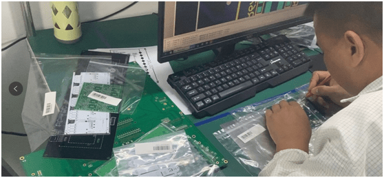
Electronic Components Checking
UETPCB will do another step before assembly, that’s components checking, our engineer team will check the components package, value, qty, Footprint, part number, etc. if matched the BOM and the PCB board. there exist any mistakes we will solve with a customer before starting assembly.
Actual PCB Assembly Process steps
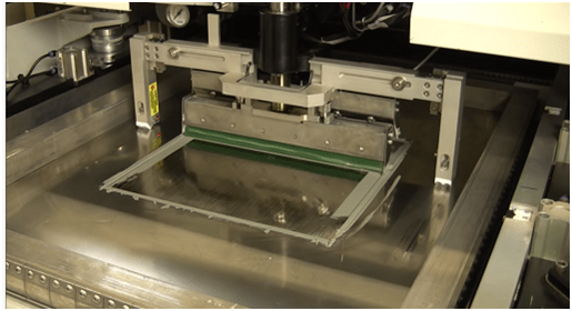
Solder Paste Printing
The solder paste printer uses stencils and squeegees to apply solder paste(a paste of small grains of solder mixed with flux) to the pads on the board.
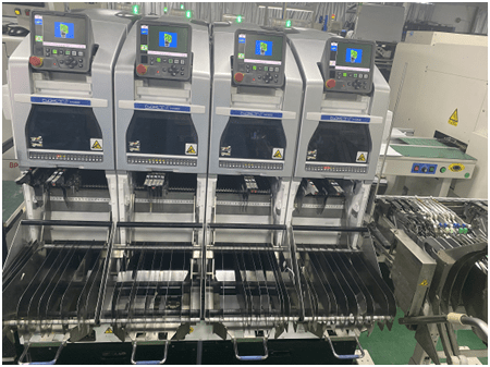
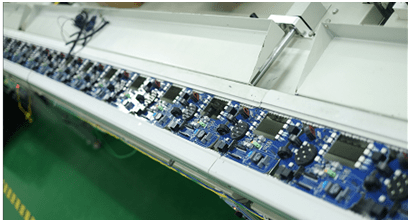
Placing of Components
This stage of the PCB assembly process is now completely automated. The pick and place of components such as surface mount components, which were once done manually, are now executed by robotic pick and place machines. These machines accurately place the components in the pre-planned areas of the board.
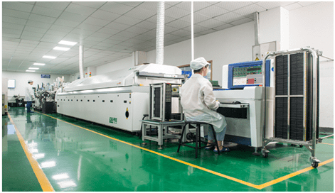
Reflow Soldering
Once the solder paste and surface mount components are all in place, they need to remain there. This means the solder paste needs to solidify, adhering components to the board. To accomplish this, the assembly with the solder paste and the components on it can pass through a conveyor belt, which moves through an industrial-grade reflow oven. The heaters in the oven melt the solder in the solder paste. Once this meeting can do, the assembly does again move in the conveyor belt and expose to a series of cooler heaters. The purpose of these coolers is to cool down the melted solder and to attain a solidified state.
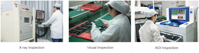
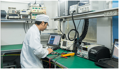
Inspection
After the reflow process, the PCB is subjected to inspection to check for its functionality. This stage helps identify poor quality connections, misplaced components, and shorts due to the consecutive movement of the board during the reflow process. The PCB manufacturers employ several inspection steps such as Visual Inspection, automatic optical inspection, and X-ray inspection to examine the functionality of the board, recognize lower-quality solder, and identify any potentially hidden problems.
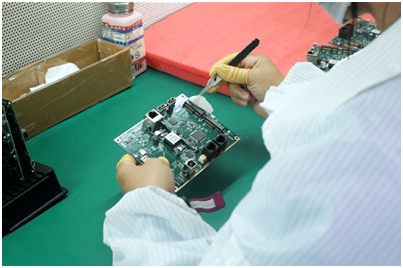
Through-Hole Component Insertion
Some types of PCBs require the insertion of through-hole components in conjunction with the usual SMD components. This stage can devote to such component insertion. For this, the plated-through hole does create with the help of which PCB components pass signals from one side of the board to the other. The PCB through-hole insertion is usually Manual Soldering or Wave Soldering to achieve the results.
Wave Soldering
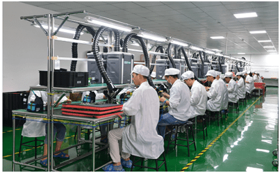
Manual Soldering
Final Inspection and Functional Test/ IC Programming
After the soldering step of the PCBA process does finish, a final inspection will test the PCB for its functionality. This inspection is known as a “functional test”. The test puts the PCB through its paces, simulating the normal circumstances in which the PCB will operate. Power and simulated signals run through the PCB in this test while testers monitor the PCB’s electrical characteristics.
Functional Test
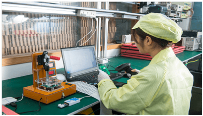
IC Programming
Cleaning and Packing
As the soldering process leaves some amount of flux residues in PCBs. We need to clean these residues off. Because after a few months, the flux residue starts to smell and feel sticky. It also becomes somewhat acidic and can damage solder joints over time. It is crucial to clean the assembly thoroughly before shipping the final board to a customer.
For this, the PCBs washes in deionized water. After the cleaning process, the board dried thoroughly utilizing compressed air. The PCB assembly is now ready for the customers’ check and inspection. After cleaning, a quick drying cycle using compressed air allows the finished PCB to be packaged and shipped.
Cleaning
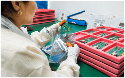
Packing
Types of pcb assembly technology.
Compared to through-hole mounting processes, surface mount processes are highly automated. And in pcb assembly, smt reduces labor costs and increases productivity. Also, SMD can be one-fourth to one-tenth of its size and weight and one-half to one-fourth of the cost of an equivalent through-hole part.
SMT: SMT stands for “Surface Mount Technology.”
Among the types of pcb assembly, SMT components are very small in size and can be used in various packages. And surface mount technology (SMT) is more effective for the complex PCB assembly process. And with the increasing complexity of electronic devices and PCB designs, the industry is also adopting the hybrid assembly type. The hybrid PCB assembly process combines THT and MMT, as the name suggests. SMT component assembly can be very time-consuming and difficult for humans. Therefore, it is mostly done by automated pick-and-place robots.
The PCBA steps followed for SMT assembly are detailed below.
Solder Paste Printing: Referring to the design template, the solder paste can apply to the board by a solder paste printer. This allows the solder paste to left exactly where the components should mount in the pcb assembly.
Component Assembly: Component placement is automated in SMT assembly, with robotic pick and place mechanisms picking and placing components.
Reflow Soldering: After component mounting, the PCB is placed in a furnace where solder paste melts and is deposited around the component.
THT: THT stands for “Through-Hole Technology.”
This applies to components with leads and wires, such as resistors, PDIP ICs, transformers, transistors. The assembly of THT components is typically done by hand soldering, and it is very simple.
The PCBA steps followed for THT assembly are detailed below.
Component Assembly: This process requires manual installation by an experienced engineer. The component placement must comply with the through-hole placement process regulations and operational standards to ensure a high quality end product. Engineers should follow THT standards and regulations to produce the best possible pcb.
Inspection and Component Correction: The PCB board can match the design shipping frame to ensure accurate component placement. If people find any component misassignments, they can correct them only at that time. Corrections are easier before soldering to correct component placement at this stage.
Wave Soldering: THT uses wave soldering to cure the solder paste and maintain the component at a particular location.
About Us
Hope the above one stop pcb assembly steps can help you have gained a good understanding of the basic steps involved in the PCB assembly process, for more PCB assembly processes and technology, please refer to other pages on our site, any questions you can send email to [email protected]