
Printed circuit boards (PCBs) are essential parts of many modern smart appliances, linking individual elements through a complicated network of circuits. With an intense emphasis on decreasing problematic resource supply chain concerns and technological improvements, global consumption of printed circuit boards has risen significantly, enhancing the need to solve PCB defects. Over the last eight years, the world’s total shipments of circuit boards have surged by a median of over $3.7 billion each year. In 2018, global PCB sales were estimated to be at $82 billion.
With that much capital invested in PCBs and the important function they perform in a variety of power devices and box construction assemblages, PCB failure is a big area of tension for many businesses. Next, let’s learn about PCB defects and how to deal with them.
What are PCB defects or PCB failures?
A variety of factors can cause PCB defects. The final effect of a PCB defect seems to be that the PCB is no longer functional. PCBs are utilized in a variety of electronics, including smartwatches, aircraft, telescopes, and hospital instruments. Therefore any pcb problems must be quickly identified and remedied. By understanding why PCB defects occur, any organization trying to keep its electronics functioning smoothly may better handle it and even eliminate it.
How to identify faulty electronic components and PCB defects?
Various pcb defects tests are conducted to identify faulty electronic components so that any future diagnosing circuit board problems can be avoided. Sometimes the faulty piece slips into the category of new products and can cause issues. Let’s know how to identify board level and community level PCB defects so that proper functioning of the electronic components can be ensured.
Polity electronic components are identified at three different times during the stages of the project.
- Before fabrication
- During assembly
- During functional testing after a PCBA is received
Manufacturers and semiconductor companies always claim that they have removed all kinds of faulty components from the electronic circuits. However, the problem(pcb defects) is sometimes the issues still may occur. At this stage, the main responsibility is of the engineers and quality testers is to identify the faults in the components so that the potential future problems can be avoided.
How to identify pcb defects in the manufacturing process?
Manufacturers and semiconductor companies usually claim to use two ways to identify faults in the electronic board components.
Burn-In Testing – pcb defects
It is the process in which the heating technique is used and all the components are heated. Under very intense heat, the components start burning. Their efficiency to run in the hot environment is checked at this stage. Many components that have a short lifespan or less ability to withstand fluctuation in the temperature are removed.
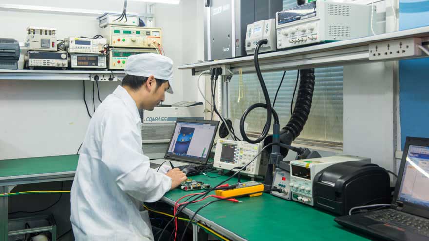
This is a high-volume process which simply means that it is conducted for a large volume of products at the same time. However, if you want to know the process that identifies the diagnosing circuit board problems during the assembly process, then you should understand what is in-circuit testing. Let’s know more about in-circuit testing and how it can identify PCB defects.
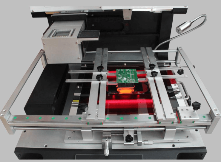
In-circuit testing – pcb defects
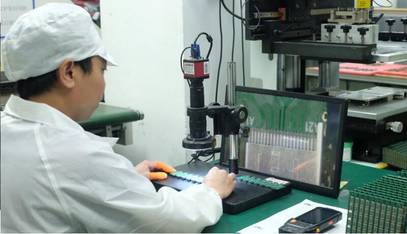
Both flying probe machines and bed-of-nails testers are used to determine problems with printed circuit board components. In this process, the original components of the printed circuit board are tested for voltage and temperature fluctuations, and the probe machine provides such an environment.
Design values and the ability to withstand different environments are checked through electrical measurement standards. The comparison of these measurements with the intended design values gives a clear idea of the efficiency of the components. The pro tip in this regard is to place test points on the PCB so that the components can easily be identified and checked for in-circuit testing.
If the actual measurements and the ones estimated from the design do not match, it simply means that there can be a fault in the respective electrical components. At this stage, further testing is conducted to check out what kind of PCB defects are expected and whether it is a board-level or component-level failure.
How to identify faulty components during board bring up?
It can be harder to detect a damaged operational efficiency during board bring-up. A single defective element can enable a circuit to perform defectively or not at all, but it’s not always clear whether the breakdown is attributable to a device. A manufacturing flaw, a fabricating error, an improper footprint, or an improved process performance could all be to blame.
Designers must explore along the faulty circuit and attempt to pinpoint the exact place where the fault happened in this sort of product examination and troubleshooting procedure. It’s possible that the element that looks to be bad on a finished circuit isn’t the one that’s causing the issue; it might be another item along the transmission route.
So you can notice that the process of identifying the pcb board problems from the board is quite difficult. You will have to know the efficiency of all the components. In case all the components are working perfectly, you can expect that the pcb problem is with the designing and manufacturing of the product.
The causes of PCB defects (PCB defect list)
The most common causes of PCB defects and PCB failure include their exposure to excess heat and humidity, human error, soldering issues defective footprint, and burnt components.
Let’s study the effects of PCB defects in detail.
PCB Defects
PCB Defects like a short circuits, misaligned layers, and dissipative floor surfaces can cause a loss of problems with the components of the PCB boards. However, some kinds of defects are only temporary and can be removed by making simple adjustments. However, other side effects are long-term and can cause permanent damage to the PCB board.
For example, a short circuit is a temporary problem that can easily be fixed but catastrophic defects are usually long-lasting. So diagnosing circuit board problems is mandatory. Here it is important to mention that PCB is extremely sensitive to electric charges. Even the smallest fluctuation in the charge can destroy the PCB.
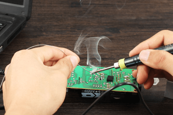
Soldering Issues
Solder is an important component of the PCB manufacturing system. It’s just what keeps an element’s connection with the circuit intact, yet it can become polluted and cause a circuit malfunction. The solder can become sensitive and cause sparking if there is too much humidity in it. So solder paste printing defects are also included in PCB defects.
But it’s not just solder uniformity to be concerned about; it’s also an installation mistake. There are a few different sorts of solder flaws, each of which has a different effect on the board.
- Opens
- Soldering too much
- Displacement of parts
- Cold joints
- Bridges made of solder
- Splashes and webbing
- Pads that have been raised
These PCB problems related to soldering flaws may usually be remedied with sufficient instruction and practice for your manufacturing.
Burnt Components
Extreme heat or component failure can cause internal components to burn out and eventually cause the entire PCB to fail. We can avoid the problems that can occur with burned components due to heat by using large spaces within the board. This way the heat can be easily dissipated.
Keep in mind that the temperature tolerance of the PCB is a maximum of 170 degrees Celsius. Any increase in temperature beyond this will destroy components.
Environmental Factors
Circuit boards are also susceptible to external influences. PCBs can expand due to humidity and heat, culminating in bending and possibly broken welded junctions. This is why PCB manufacture is often done in a climate-controlled setting with an acceptable degree of moisture.
In addition, foreign material that comes into contact with a board can have negative consequences. Dust, hair, liquid, and fibers are some of the major components that can also interact with the components and retard their performance and functionality.
Human Error
Anyone can cause a PCB error. When it comes to PCB errors, the main people involved in making some kind of mistake that leads to component failure include designers, manufacturers, quality inspectors, assemblers, and engineers.
Sometimes they poorly install the components, do not focus on the excessive spacing among the components or they do not proceed with excellent soldering. However, all types of human errors require a bit more work and then they can be rectified.
However, if all the research and checks have been done, no problem is still found. This means that the PCB problem may lie in the footprint of the PCB. Let’s learn more about what is PCB footprint? And how it can cause PCB problems in the functionality of the PCB.
PCB Footprint
If the inspection expert is successful in finding out that the problem is with the PCB footprint. Then it means that the whole lot is faulty. To solve this kind of faulty component problem, research, examination, and detailed scrapping work are required.
Because many elements are meant to be drop-in equivalents, the occurrence of an erroneous pinout with corresponding ground arrangements is rare. Use an electronic components search engine to locate certified patterns, design diagrams, and procurement information for your model to verify you’re always using proper footprints.
Wrapping Up: Fixing PCB Defects and PCB Failures
Now that you know all of the causes that are involved in PCB failures. You can easily get rid of the problem by identifying the issues and solving them. It is important to do extensive research before you start solving the problem of PCB failures. You need to contact a company like UETPCB, which knows the ins and outs of PCB defects. So such pcb manufacturers can design solutions and deliver error-free products.
UETPCB is a Chinese PCB manufacturer with years of experience. They are also the finest PCB assembly manufacturer in China. They have over 15 years of expertise in the China PCB manufacturing and China PCB assembly industries as an outstanding China PCB manufacturer. And you should be capable of solving any difficulty you come across in the PCB field.