
Rotating components have to transfer electrical power between the rotating and stationary components. At the same time, this transfer is possible with wiring; challenges arise, such as wire twisting or entanglement. It may cause failure and may present many more issues as well.
Slip rings are the best possible solution in such a case. Do you want to know how? Today we will discuss slip rings, their importance, and more. Let’s know them in detail.
What is a PCB Slip Ring?
A PCB Slip Ring helps transfer electrical power between stationary and rotating components while maintaining continuous rotation. They don’t need specialized wiring systems for power transfer.
Instead, a simple transfer of current is sufficient between the stationary and rotating components.
The basic arrangement includes:
- The stationary section connects the external power or signal source.
- The rotating section ensures the electrical connection is transferred to the rotating equipment.
- The contact system confirms electrical contact during rotation.
- PCB conductive structure provides an arranged electrical path.
- Insulation separates individual circuits and prevents unwanted connections.
How Does PCB Technology Help in Slip Ring Designs?
PCB technology is very helpful in the compact design and transfer of the energy between the stationary and rotating components.
Here are a few options often used here.
PCB Substrate
The PCB substrate provides electrical insulation between circuits and provides mechanical support. You should choose the PCB circuits according to the application requirements, such as:
- Operating temperature
- Mechanical strength
- Electrical insulation
- Dimensional stability
- Required board thickness
- Environmental conditions
Copper Conductive Paths
Copper is one of the best electrical conductors often used in electrical circuits. PCB uses copper conductive paths for slip rings to ensure seamless electrical conduction.
There are a few crucial design factors used in the copper conductive paths, such as:
- Copper thickness
- Conductor width
- Rated current
- Electrical resistance
- Heat generation
- Circuit spacing
For higher currents, you should consider wider or greater copper thickness.
Conductive Rings and Contact Areas
Conductive rings interact to provide seamless electrical transfer between components. They offer a conductive path and provide the contact areas.
There are a few key considerations:
- Conductive path geometry
- Contact area
- Contact pressure
- Electrical resistance
- Wear characteristics
- Circuit separation
Insulation Between Circuits
Do you want to avoid short circuiting or electrical interference? Insulation between circuits is then the most essential factor here. You should consider the insulation between the circuits and make sure there is no contact to reduce the risk of sudden failure.
The design should provide:
- Adequate circuit spacing
- Electrical isolation
- Suitable insulating material
- Appropriate voltage clearance
- Separation between power and sensitive circuits
PCB Layout and Manufacturing
PCB layout and manufacturing determine the positioning of conductive paths, connection points, mounting features, and other elements. The compact structure of slip rings must ensure seamless electrical conduction between components.
Key PCB Design Considerations for PCB Slip Rings
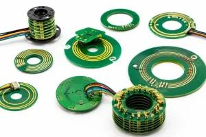
There are a few key factors to consider when designing the PCB circuits for the slip rings.
Circuit Layout
Circuit layout determines the comprehensive structure of the PCB designs. It must be arranged within the circuitry with adequate spacing and layout.
Here are a few circuit layout options to consider:
- Number of electrical circuits
- Circuit arrangement
- Connection points
- Electrical clearance
- Mounting locations
- Available PCB area
Current Capacity
Current capacity matters as it helps understand how much electrical load each pathway can handle safely. If the conductor is undersized, heat dissipation can be insufficient, leading to overheating.
Here are a few more things to consider when choosing the current capacity.
- Continuous current
- Peak current
- Copper thickness
- Trace width
- Electrical resistance
- Heat dissipation
Signal Integrity
When a slip ring carries signals, signal integrity is crucial as well. Factors such as electrical noise, contact resistance, interference, and poor circuit layout can affect signal integrity.
Design related to signals should take the following considerations into account.
- Signal type
- Signal frequency
- Circuit separation
- Grounding
- Shielding
- Contact resistance
Board Thickness
Board thickness is also crucial in many cases, especially when you need extended durability. Thicker boards offer greater durability; however, they may take up more space.
When choosing the board thickness, you must consider factors such as:
- Available installation space
- Mechanical strength
- Overall slip ring thickness
- Manufacturing capability
- Structural requirements
Mechanical Dimensions
Electrical performance is not sufficient. Instead, there should be a proper assembly of the components inside the given compact PCB structure. Here is the list of factors to consider.
- Outer diameter
- Inner diameter
- Overall thickness
- Mounting-hole locations
- Shaft dimensions
- Cable exit positions
PCB Slip Ring vs. Traditional Slip Ring
| Feature | PCB Slip Ring | Traditional Slip Ring |
| Structure | PCB-based conductive structure | Conventional metal ring assembly |
| Profile | Compact designs are possible | Depends on construction |
| Circuit Arrangement | PCB-based layout | Metal ring arrangement |
| Power Transmission | Yes | Yes |
| Signal Transmission | Yes | Yes |
| Customization | PCB and mechanical design | Ring, brush, and mechanical design |
| Circuit Density | Can be high in compact designs | Depends on ring configuration |
| Manufacturing | PCB production plus assembly | Mechanical and electrical assembly |
How to Choose the Right PCB Slip Ring
When choosing the right PCB Slip rings, you should consider the factors below.
Determine the Number of Circuits
First, determine the number of circuits passing through the rotating interface. It should include current circuits and low-level signal circuits.
There are a few aspects to consider regarding the number of circuits.
- Power circuits
- Ground connections
- Control signals
- Sensor signals
- Communication channels
- Spare circuits
Check Rated Current
Current and voltage are the two most important aspects that should match under all conditions. The mismatch can result in failures and damage.
The selection process of the current should evaluate:
- Continuous operating current
- Peak current
- Required safety margin
- Conductor capacity
- Heat generation
Confirm Rated Voltage
Voltage compatibility is essential. Make sure rated voltage matches the slip rings and installed systems.
You should consider the following aspects of voltage.
- Operating voltage
- Maximum voltage
- Insulation requirements
- Circuit spacing
- Electrical clearance
Consider Rotational Speed
You should match the rotational speed of the slip rings with the required conditions. A slow intermittent rotation of the slip rings may not be suitable for the high speed continuous operations.
Here are a few types of rotational speeds to consider.
- Normal rotational speed
- Maximum rotational speed
- Rotation direction
- Continuous or intermittent operation
- Expected operating cycles
Identify Signal Requirements
Power and signals have different requirements. If a circuit delivers a high-quality signal but electrical interference is present, it may not operate efficiently.
Moreover, you have to consider the signal types, such as:
- Analog signals
- Digital signals
- Sensor signals
- Communication signals
- High-frequency signals
- Combined power and signal transmission
Measure Available Space
You should measure the space available before choosing the PCB design. Even if the electrical requirements are correct, the physical dimensions may not be suitable, causing the circuit to fail or experience increased stress.
You should measure.
- Outer diameter
- Inner diameter
- Overall thickness
- Mounting dimensions
- Shaft dimensions
- Cable routing space
Consider the Operating Environment
The operating environment has a huge impact on the durability and performance of the PCB circuits. It can damage the mechanical components and may cause failure if not managed properly.
Here are a few factors to consider regarding the environmental conditions.
- Dust
- Moisture
- Oil
- Vibration
- Temperature variation
- Chemical exposure
- Continuous operation
Evaluate Service Life
Service life varies from one PCB to another depending on how you maintain or manage the circuits. However, you should choose PCBs based on their service life. If your use is occasional, the service life may differ. If your use is continuous, service life is also different.
You should choose the PCB based on the following conditions.
- Operating cycles
- Rotation frequency
- Duty cycle
- Contact wear
- Maintenance requirements
- Expected service life
FAQs
- When is a custom PCB slip ring required?
A custom PCB slip ring is required to meet demands for circuit count, current, voltage, signal type, outer diameter, inner diameter, thickness, mounting configuration, rotational speed, or environmental conditions.
- Can PCB slip rings be used for high-speed rotation?
Yes. PCB slip rings can be used in high-speed rotation systems, but they must meet suitable contact systems, materials, mechanical construction, electrical requirements, and an expected service life.
- What applications commonly use PCB slip rings?
PCB slip rings are commonly used in robotics, rotary tables, packaging machinery, automation equipment, rotary sensors, camera systems, and medical equipment.
- How does PCB thickness affect a slip ring?
A high PCB thickness can help conduct high currents and withstand greater mechanical stress compared to thin PCB circuits. However, it may be expensive. You should consider suitability and other cases in such conditions.
- How does a PCB slip ring maintain electrical contact during rotation?
A PCB slip ring uses conductive pathways to maintain electrical contact during rotation. It uses contact or brush systems to ensure electrical transmission.
Conclusion
PCB slip rings are advanced, compact solutions that eliminate wiring and other failure-prone components. They help maintain the electrical transfer without interrupting the continuous movements of the components. However, when choosing PCB slip rings, you must focus on the PCB substrate selection, copper thickness, conductor width, circuit layout, insulation, board thickness, and mechanical dimensions.
If you are looking for PCB-related components, contact UETPCB. We have a wide range of excellent tools with high performance, compact design, and affordable prices. Contact our experts to get a quote for your PCB products.