
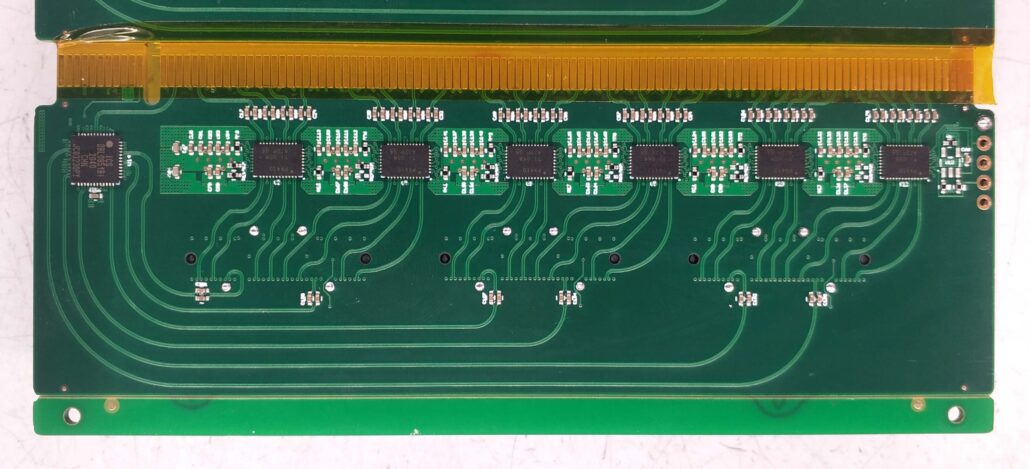
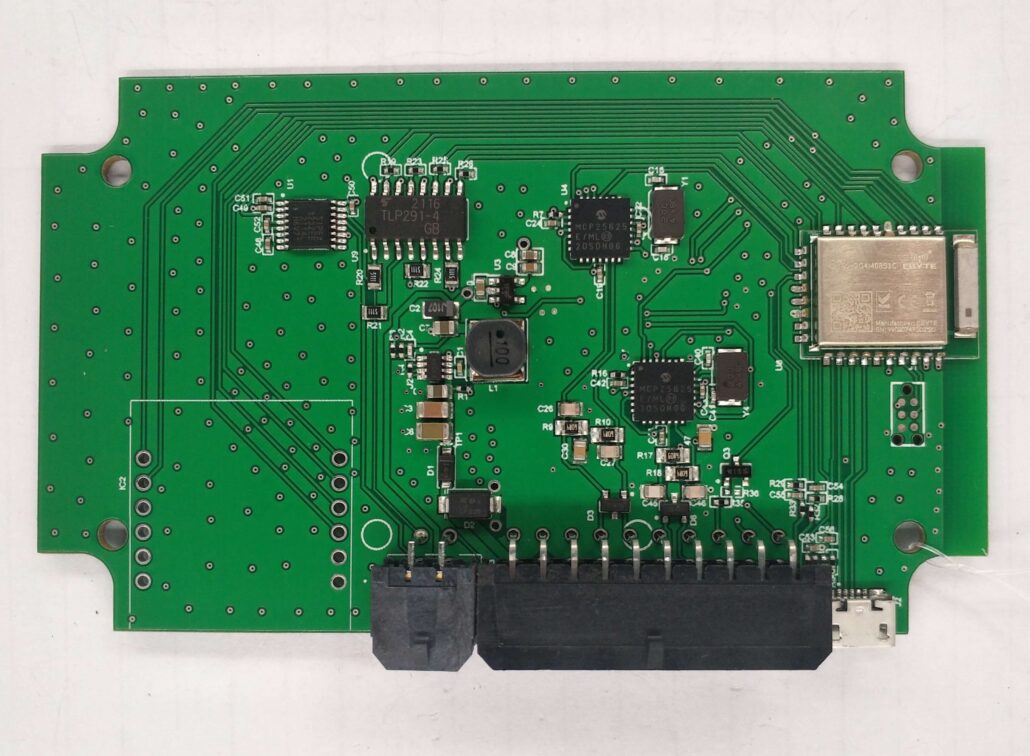
The PCB we see daily comprises a pcb solder mask, silk screen layer, copper wire, and other parts. The solder resists layer is essential in controlling the role of the reflow soldering process. Generally speaking, we call the feature of the printed circuit board greased with green oil as the pcb solder mask.
The solder resists process in the printed circuit board is to screen print the printed circuit board. In order to protect it from UV radiation during exposure, the printed board’s pad is covered with a photographic backing. Additionally, solder is more firmly adhered to the printed board surface and resists the protective layer after being exposed to UV light.
The difference between solder resists and flux layer.
The paste mask industry is known as “stencil” or “steel plate.” This layer is a distinct stencil and does not appear on the printed board. Using this stencil, solder paste is applied to the SMD pads during the automatic soldering process of SMD assemblies. The SMD pads are hollowed out at the top, and the shape of the hollowing is generally the same as the SMD pads, with a slightly smaller size.
PCB solder mask
PCB solder mask: The area of the board that has to be greased is this one. Since the output is negative, the solder mask on the part has no real impact on the green oil. Instead, it is silvery white and tinned. (In other words, tin plating rather than green oil will be present when a solder mask is present.)
Flux layer
Paste mask: is the machine to be used when patching corresponds to all the pads of the SMD components. The size and top layer/bottom layer are the same and are used to open the stencil leakage of tin.
Point: two layers are on the tin soldering with, does not mean a tin, a green oil. The layer of green fat is not mentioned after that. As long as a certain area is on the layer, does it mean that this area is on the insulation of green oil? I have not yet encountered such a layer, sorry! We draw the PCB board. The pads on the default case have a pcb solder mask. Therefore, the pads component of PCB boards is produced using silver-white solder rather than green oil, which is not unusual. However, we only sketch the top or bottom layer of the PCB board alignment, not the folder layer. But the PCB on the alignment part of the board is on a layer of green oil.
- The pcb solder mask means a window on the whole piece of the solder resists green oil. The purpose is to allow soldering!
- The area on the green oil does not by default, have a pcb solder mask!
- Apply a solder mask material to SMD packaging! SMT packaging comprises a top layer, a top solder layer, a top pasta layer, and a top soldier layer that is larger than a circle.
- Tin or gold plating: To provide the desired effect, the component coated in the solder layer is given a tinned finish, and the matching solder layer portion receives a copper skin.
The role of the pcb solder mask
The elemental composition of the printed circuit board is the pads and vias. PCB solder mask, text printing part. The pcb solder mask is the yellow, red, black, green, or other color parts we see. Some boards are yellow solder resist layer. The role of the solder resists layer is to prevent the position that the solder connection should not solder on. Reflow soldering is achieved by the pcb solder mask. On the whole side of the board, after rolling hot tin water, no solder masking of the bare circuit board will be soldered with tin, while the part with a solder masking layer will not be tin.
Solder resist is a major cause of PCB defects.
Solder resist adheres well to the surface, but narrow sections can still peel off. IPC has developed a test method in which a tape with a specific adhesive is stuck to the board and removed from the board. We can inspect the tape to see if anything, conductive or non-conductive, has come off. Of all the possible defects, more boards failed the tape test than any other board.
The four primary types of solder mask
The solder resists layer prevents conductive solder bridging between various electronic components. In essence, it blocks short circuits. The different PCB solder mask layers are listed below.
Top and bottom masks:
The electronics engineer knows the various openings. He knows what has been added by ink, epoxy, or film technology. With the aid of a verified alignment, he may solder the components’ pins on the board. Additionally, the layout of conductive traces is visible on the board’s top. Call these top staring. Lower is the bottom mask.
Epoxy Fluids:
For an inexpensive option, pick an epoxy fluid. Thermoset polymers are used in a variety of ways. Screen printing is a printing technique. A woven mesh supports the ink-blocking pattern. For handling ink, the mesh may produce an open area.
Liquid inks can be photographed and imaged:
We supply pcb solder mask as ink formulations. The ink can be sprayed into the PCB. The pattern can then be discovered and expanded upon. It’s crucial to keep in mind that the procedure and the liquid ink composition are used. This requires a clean environment free of contaminants and particles. One can remove it after exposing it to UV light. This is done through a high-pressure water spray called a developer.
Dry Film Photographic Imaging:
This solder masking is applied by vacuum lamination. Making apertures and soldering the components to the copper pads is possible after development. In addition, tin is used to maintain the copper circuit. The dry film is then removed.
The process of pcb solder mask
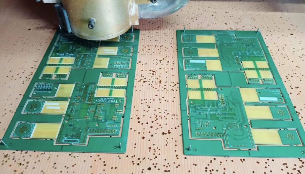
Pre-baking
Pre-drying is done to get the solder resist coating to a non-stick state by evaporating the solvent from the ink. For the different ink, the temperature and time of pre-drying are different. Pre-drying temperature is too high, or drying time is too long, will lead to poor development, reducing the resolution. Pre-drying time is too short or the temperature is too low, the exposure will adhere to the negative. In the product, the solder resists film will be eroded by the sodium carbonate solution, causing the surface to lose luster or solder resist film expansion off.
Exposure
Exposure is the key to the entire process. If overexposure, due to light scattering, graphics or line edge of the solder resist film and light reaction to generate a residual film. This decreases the resolution, developing graphics with more minor, thinner lines. If the exposure is insufficient, the result is the opposite of the above. The development of the pictures becomes larger, thicker lines.
This scenario may be reflected in the test: extended exposure time and negative tolerance for measured line width. Short exposure duration, positive tolerance for the observed linewidth. In the actual process, you can use the “light energy integrator” to determine the best exposure time.
Ink viscosity adjustment
The viscosity of liquid photoresist ink is mainly through the hardener, the main agent ratio, and the amount of diluent added to control. If the amount of hardener added is not enough, it may produce an imbalance in the characteristics of the ink.
What is the meaning of pcb solder mask open window?
The area of the printed circuit board that needs to be greased is referred to as the PCB solder mask. This solder mask has a negative output, so when the mask’s shape is projected onto the board, it does not cover the copper skin but rather the green oil solder mask.
The process requirements of the white solder mask
In order to control solder flaws during the reflow process, the solder resists layer is crucial. The air gap or space around the pad features should be kept to a minimum by PCB designers.
The white solder mask many process engineers prefer layer over separating all pad features on the board. But closely spaced components will need additional attention given to the pin spacing and pad size.
While not partitioning the solder mask openings or windows on the four sides of the pad may be acceptable. But controlling the solder bridges between component pins may be more difficult. Many companies offer a white solder mask for the BGA pcb solder mask. In order to prevent solder bridges, it does not touch the pads but rather covers any features in between. Solder resist is the layer that covers the majority of surface mount PCBs. However, if the pcb solder mask thickness is greater than 0.04mm, the solder resistance layer is deposited and may interfere with the application of solder paste. A low-profile light-sensitive white solder mask is necessary for surface-mount PCBs, especially those with closely spaced components.
PCB solder mask window
The solder resists window is the size of the part of copper exposed at the location where soldering is required. That is, not covering the size of the ink part. The term “cover line” describes the amount and size of solder resist oil used to cover the line section. Covering the line distance is too small in the production process will cause the exposed line.
PCB solder mask open window reason
- Aperture windowing: Many customers do not need ink plugging holes. The ink will fall into the pit if the window is not opened. (This applies to tiny holes) If the large hole plugged in ink into the customer can not be on the key. In addition, if it is a chemical gold plate, you must also open the window
- Customers must weld and apply surface treatments (gold/spray tin, etc.) to copper (PAD) when the window is open.