
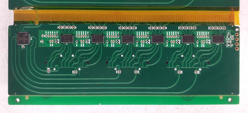
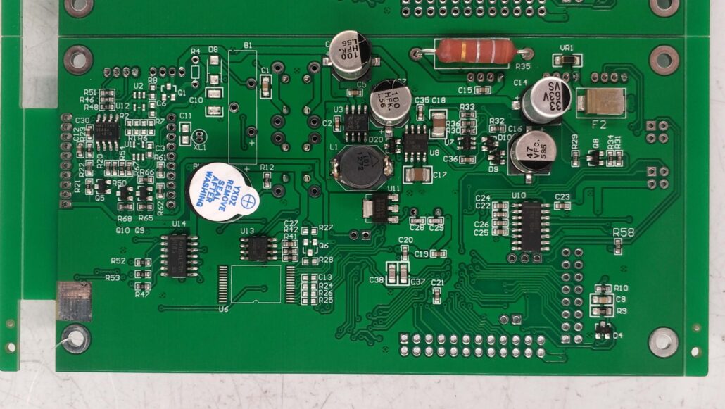
Immersion tin PCB is printed circuit board tinning belonging to one of the PCB Surface Finishes. It’s not the same as Hot Air Solder Leveling (HASL). Immersion Tin PCBs are meant to make SMT and chip packaging procedures easier. HASL has process limitations in PCB Surface Finishes. China immersion tin pcb finish as an alternative to HASL, immersion tin is mainly attached to the copper circuit surface through the exchange between copper and tin. Its primary function is to protect copper circuits from oxidation. And because tin looks white, so also known as “white tin.” Also, dipping tin is the cheapest way to process all PCB surface finishes. Therefore, it is very popular among designers.
Advantages of the immersion tin pcb finish
- Excellent conductivity and solderability, can be soldered many times
- The tin layer in the sink does not contain lead and does not pollute the environment
- Simple process, easy to rework, low cost
- Long storage period (0.6-1.5 years)
- Suitable for small pitch/BGA/small component placement
- Smoother original surface
Disadvantages of immersion tin pcb surface treatment
- Tend to form whiskers, leading to short circuit problems in connections
- Thiourea (carcinogen) is used in the process
- Not good for PTH
- May damage solder resist layer
- Difficult to measure the thickness
China immersion tin PCB VS HASL
Two joint surface treatment procedures for printed circuit boards are HASL and immersion tin. However, most people are unable to discern between the two. The parallels and contrasts between the two are then discussed.
Similarities.
Surface treatment processes such as HASL and immersion tin meet the standards for lead-free soldering.
Differences.
1. Process flow
HASL: Pre-treatment – Tin spraying – Testing – Forming – Appearance inspection.
Immersion tin: Testing – Chemical treatment – Immersion tin – Molding – Appearance inspection.
2. Process Principle
HASL is mainly to invade the PCB board into the molten solder paste directly. A dense tin coating will be produced on the copper surface of the PCB after the hot air leveling.
Immersion tin is mainly used to form a thin layer of tin on the PCB surface by a displacement reaction.
3. Physical properties
Because HASL uses only pure tin in the manufacturing process, the surface is easy to clean and can be stored for a year at room temperature. The thickness of the HASL tin layer is about 1um-40um, and the immersion tin pcb surface structure is dense, complex, and not easy to scratch. It is not easy to have surface discoloration problems during the welding process.
The thickness of immersed tin is about 0.8um-1.2um. The surface structure is looser and softer, and it is scratch-prone. Because the chemical reaction in the immersion tin is complex, cleaning it is difficult. Can store it at room temperature for six months to a year.
4. Appearance characteristics
HASL – The surface is bright and beautiful.
Immersion tin – light white surface, no luster, easy to change color.
How to apply immersion tin?
The steps of tin dipping pcb are as follows.
1. Cleaning
This is the first step in the plating process. Immerse the board in an acid solution to remove oil, grease, and other surface impurities. Rewash the surface with water to remove any remaining cleaning solution and surface residues. This step improves the efficiency of the plating process.
2. Micro-etching
China immersion tin pcb takes a second dip in a solution containing sulfuric acid (H2SO4). This acid provides roughness to the copper layer structure of the pcb and allows it to bond with the tin layer. We clean the surface of the immersion tin pcb again to ensure no residue.
3. Prepreg
In the prepreg, rinsing the PCB with acid prevents premature oxidation of the copper surface. This provides a good framework for the deposition of tin.
4. Tin dipping
The board is immersed in a solution consisting of tin cations to accelerate the chemical reduction process. The tin ions reduce the copper metal. This will form a thin, flat layer of tin on the copper solder pad.
5. Cleaning
In this step, the immersion tin PCB can wash with warm water to remove plating salts and to prevent staining when drying. If not rinsed properly, the board will appear dull and shiny.
6. Drying
After cleaning, it is vital to dry the board. Drying removes moisture from the surface. We can do this by baking in an air dryer or a warm oven. The key is to make sure that the baking time and operating temperature.