
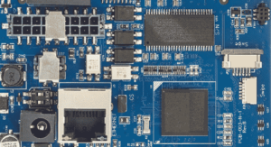
As we all known that the PCB is the acronym of Printed Circuit Board, a mechanical base that contains tracks and footprints reflecting the schematic of the design. As the foundational building block of most electronic devices, the Printed Circuit Boards (PCBs) can be used as the foundation on which all of the other electronic component are assembled onto from a simple single board used in your car key to high precision and high-speed circuit boards used in computer.
There are 5 things help you make PCB manufacturing and PCB assembly (PCBA) better.
- 1. PCB Manufacturing and PCB Assembly Process
- 2. Some Ways to Control Quality in PCB Process
- 3. Short Checking & Quality Identify for PCB
- 4. Conformal Coating
- 5. Evaluate A PCB Manufacturer
1. 9 Steps to Create Effective PCB Manufacturing and PCB Assembly Process
Before the Assembly Process
-
Design for Manufacturability (DFM) Check
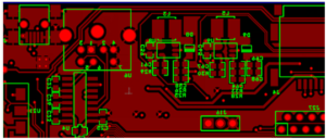
Then what’s the DFM CHECK? before the actual assembly process, manufacturers thoroughly check the PCB design file to check the functionality, and manufacturability. This stage, we called DFM, checks design specifications of a PCB, analyze any missing, redundant or potentially problematic features. The stage helps detect design errors, and allows the designers to instantly clear all the flaws, which in turn leads to successful production.
-
Electronic Components Checking
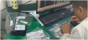
UETPCB will do another step before assembly, that’s components checking, our engineer team will check the components package, value, qty, Footprint, part number, etc. if matched the BOM and the PCB board. there exist any mistakes we will solve with customer before start assembly.
Actual PCB Assembly Process Steps
-
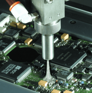
Solder Paste Printing
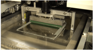
The solder paste printer which is designed to apply solder paste (a paste of small grains of solder mixed with flux) using a stencil and squeegees to the appropriate pads on the boards.
-
Placing of Components
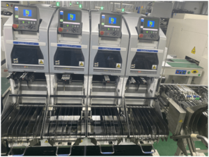
This stage of PCB assembly (PCBA) process is now completely automated. The pick and place of components such as surface mount components, which were once done manually, are now executed by robotic pick and place machines. These machines accurately place the components to the pre-planned areas of the board.
-
Reflow Soldering
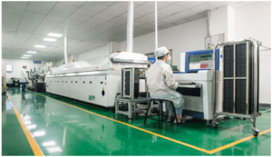
Once the solder paste and surface mount components are all in place, they need to remain there. This means the solder paste needs to solidify, adhering components to the board. To accomplish this, the assembly with the solder paste, and the components on it is passed through a conveyor belt, which moves through an industrial grade reflow oven. The heaters in the oven melt the solder in the solder paste. Once this melting is done, the assembly is again moved in the conveyor belt, and exposed to a series of cooler heaters. The purpose of these coolers is to cool down the melted solder, and to attain a solidified state.
-
Inspection
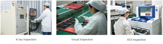
After the reflow process, the PCB is subjected to inspection to check for its functionality. This stage helps identify poor quality connections, misplaced components, and shorts due to the consecutive movement of the board during the reflow process. The PCB manufacturers employ several inspection steps such as Visual Inspection, automatic optical inspection, and X-ray inspection to examine the functionality of the board, recognize lower-quality solder, and identify any potentially hidden problems.
-
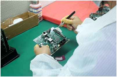
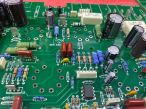
Through-Hole Component Insertion
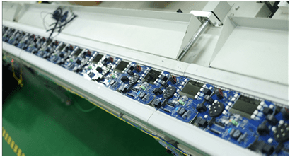
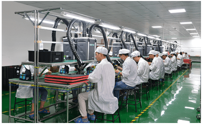
Some types of PCBs require the insertion of through-hole components in conjunction with the usual SMD components. This stage is devoted for such component insertion. For this, plated-through hole is created with the help of which PCB components pass signals from one side of the board to the other. The PCB through-hole insertion usually Manual Soldering or Wave Soldering to achieve the results.
-
Final Inspection and Functional Test/ IC Programming
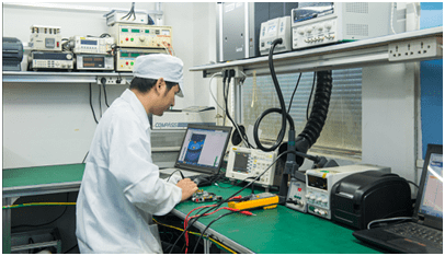
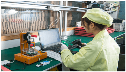
After the soldering step of the PCBA process is finished, a final inspection will test the PCB for its functionality. This inspection is known as a “functional test”. The test puts the PCB through its paces, simulating the normal circumstances in which the PCB will operate. Power and simulated signals run through the PCB in this test while testers monitor the PCB’s electrical characteristics.
-
Cleaning and Packing
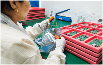
As the soldering process leaves some amount of flux residues in PCBs, it is crucial to clean the assembly thoroughly before shipping the final board to a customer. For this, the PCBs are washed in deionized water. After the cleaning process, the board is dried thoroughly utilizing compressed air. The PCB assembly is now ready for the customers’ check and inspection.
Reliability Tests in The PCB Assembly Manufacturing
PCBA manufacturing is by no means a combination of adding material procurement on the basis of SMT processing. Any problem of any material will affect the overall result of PCBA board, which requires us to have sufficient material detection ability, supplier management ability, technical analysis ability and reliability test ability.
Reliability testing is often ignored by PCB assembly (PCBA) manufacturers, who often believe that as long as the PCBA board is tested without problems, it will be accepted by end customers. However, many PCBA boards have fatal defects such as short service life and unstable use in terminal products, which are caused by the failure of PCBA factories to strictly execute reliability tests.
- Functional Testing
Functional test is used as a final PCBA manufacturing step. It provides a pass or fail determination on finished PCBA boards and validates that product hardware is no defects before they are shipped. It can check the functionality of the product anywhere from 50% to 100% of the product being shipped thereby minimizing the time and effort on the OEM to check and debug it.
- Aging Testing
The PCBA board with test function OK was placed under specific temperature and humidity conditions, and repeated switching on and off, simulated function operation, load operation and so on were carried out. The stability of the PCBA board was tested through continuous work of 24 to 72 hours. The aging test takes a long time, which makes it impossible to conduct large-scale batch operation. In the actual process, the aging test only conducts sample sampling, and the overall yield of this batch of products can be determined by the pass rate of sampling test.
- Vibration Testing
In the process of delivery to customers, many PCBA boards often have some problems caused by vibration during transportation, such as component shedding and pads cracks. Through the vibration test, the vibration effect in the transportation can be simulated effectively in the laboratory, and the hidden dangers in the PCB assembly soldering process can be gradually exposed. To avoid the poor soldering in batch PCBA boards, and improve the overall yield of delivery.
- Surge Testing
In the PCB assembly (PCBA) process, it is often OK to work under normal voltage, but a transient failure occurs in a certain power surge. Many circuit designs are not perfect. They often fail to take into account the fatal impact of instantaneous voltage or current shock on the whole circuit, which requires us to conduct the surge testing before the mass production of PCBA.
- Packaging Testing
This test is often overlooked, but may will cause a funny problem: we spent a lot of effort to make the PCBA boards perfect, but we lost in the last part of packaging and transportation. So the factory should simulate the packaging form of PCBA board to conduct appropriate drop test.
2. 5 Ways to Control The Quality of PCBA
PCB assembly is also called PCBA, and the PCBA processing process involves PCB manufacturing, components sourcing and checking, SMD assembly, DIP process, programming, testing, aging and a series of the process, If the supply chain and manufacturing chain too long. it will cause many PCBA boards happen failures. But the quality control of PCBA (printed circuit board assembly) process will avoid the most of failure of PCBA board. Therefore, most professional PCB assembly manufacturers have the quality control of PCBA (printed circuit board assembly) process to ensure the quality of PCB assembly (PCBA) service they have. It is important for PCB assembly (PCBA) to create the quality control of PCBA (printed circuit board assembly) process, and this article will provide what are some of the ways to quality control PCBA (printed circuit board assembly) process.
- 1. PCBA manufacturing
Manufacturing of PCB assembly (PCBA) is especially important to hold a pre-production meeting after receiving a PCBA order. Mainly for technique analysis of PCB Gerber files and submit design for manufacturability report (DFM) according to different customer needs. Many small manufacturers do not take this seriously, but tend to prefer it. Other important work for PCBA manufacturing is the inspection of PCB design. As the basic of PCB assembly, the PCB design decides the quality of PCBA manufacturing. It is not only easy to produce poor quality problems caused by poor PCB design, but also a lot of rework and repair work.
- 2. PCBA Components Sourcing and Checking
Components sourcing in PCB assembly (PCBA) process is also an important part of the quality control of PCBA process. Procurement channels for components need to be strictly controlled and must be obtained from large traders and original manufacturers to avoid the use of second-hand materials and counterfeit materials. In addition, a special PCBA inspection post should be set up to strictly inspect the following items to ensure that the parts are trouble-free.
PCB: Check reflow oven temperature test, whether the hole without flying line through is blocked or ink leakage, whether the PCB board surface is bent, etc.
IC: Check whether the screen printing and BOM are identical, and carry out constant temperature and humidity preservation.
Other common methods: Check screen printing, appearance, electrical measurement, etc.
- 3. SMT Assembly
Solder paste printing and reflow furnace temperature control system are the key points of PCB assembly (PCBA), which need to use the laser steel stencil which has higher quality requirements and can better meet the processing requirements. According to PCB requirements, part of the need to increase or reduce the stencil’s hole, or U-shaped hole, just according to the process requirements to make the stencil. The temperature control of the reflow oven is very important to the wetting of the solder paste and the solderability of the steel stencil, which can be adjusted according to the normal SOP operating guidelines.
In addition, strict implementation of AOI testing can greatly reduce the adverse effects caused by human factors.
- 4. DIP Process
In the DIP process, the die design for wave soldering is the key. How to use the mold to greatly improve the yield, this is PE engineers must continue to practice and summarize the process.
- 5. PCBA Board Testing
For orders with PCBA (printed circuit board assembly) testing requirements, the main test contents include ICT (In-Circuit Test), FCT (functional test), Life Cycle Testing(aging test), temperature and humidity test, drop test, etc.
3. Short Checking & Quality Identify for PCB
4 Steps of Short Checking of Circuit on PCB
Now you know the process of PCB assembly (PCBA), and how to control the quality of PCBA. After PCB fabrication and assembly, checking short and identify the quality of PCB assembly (PCBA) products can help you avoid defects during the PCBA process, and make PCB manufacturing and assembly better.
Step 1: How to Find A Short Circuit in A PCB?
Visual Inspection
The first step is to examine the entire surface of the PCB. If so, use a magnifying glass or low-power microscope. Cracks or spots in any solder should be noted. Check all through holes. If none-plated through holes are specified, make sure this is the case on the board. Poor plating through holes can cause a short circuit between layers and cause everything you have to ground, VCC or both together.
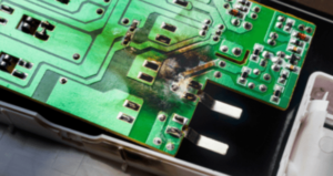
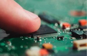
If the short circuit is really serious and causes the component to reach a critical temperature, you will actually see burn spots on the printed circuit board. They may be small, but they will turn brown instead of the normal green solder. If you have multiple boards, a burned PCB can help you narrow down the area in a particular location without having to power another board, sacrificing the search area. Unfortunately, there were no burns on the circuit board itself, just unlucky fingers checking to see if the IC was overheating.
Some short circuits will occur inside the circuit board and will not produce a burn spots. This also means that they will not be noticed from the surface. Here, you will need other methods to detect short circuits in the PCB.
Infrared Imaging
Using an infrared thermograph can help you locate areas that generate a lot of heat. If an active component is not seen away from a hot spot, a PCB short circuit may occur even if the short circuit occurs between the inner layers.
Short circuits usually have a higher resistance than normal wiring or solder pads because they have no benefit of optimization in the design (unless you really want to ignore rule checking).This resistance, along with the naturally high current generated by the direct connection between the power supply and the ground, means that the conductor in the short circuit of the PCB will heat up. Start with the lowest current you can use. Ideally, you would see a short circuit and then cause more damage.
Step 2: How to Test The Short Circuit on The PCB Board
In addition to the first step of checking a circuit board with a trusted eye, there are several other ways you can find the potential cause of a PCB short circuit.
Test with A Digital Multimeter
To test the circuit board if short circuit or not, you need to check the resistors between the different pads in the circuit. If the visual inspection does not reveal any clues as to the location or cause of the short circuit, grab the multimeter and try to trace the physical location on the printed circuit board. The multimeter approach has received mixed reviews in most electronic forums, but tracking test points can help you figure out what the problem is.
You will need a very good multimeter with good sensitivity, which is easiest if it has a buzzer function to alert you when short circuits are detected. For example, if the resistors between adjacent wires or pads on a PCB is measured, high resistors should be measured.
If the resistor between the two conductors to be measured in a separate circuit is very low, the two conductors may be bridged either internally or externally. Note that bridging two adjacent wires or pads with an inductor (for example, in an impedance matching network or discrete filter circuit) will result in very low resistance readings because the inductor is just a coil conductor. However, if the two conductors on the board are far apart and the resistance you read is small, there will be a bridge somewhere on the board
Tests Relative to The Ground
Particularly importance are short circuits involving ground through-holes or connecting formations. A multilayer PCB with an internal layer will include a return path through the assembly near the through-hole, which provides a convenient location for checking all other through-holes and pads on the board surface layer. Place one probe on the ground connection and touch the other probe on the other conductors.
The same ground connection will also exist at other locations on the board, meaning that if each probe is touched to two different grounding through-holes, the reading will be small. Pay attention to the layout when doing this, because you don’t want to mistake a short circuit for a common ground connection. All other ungrounded bare conductors shall have a high resistance between the common ground connection and the conductor itself. If the value read is low and there is no inductor between the conductor in question and the ground, the component may be damaged or short circuited.
Short Circuit Components
Checking for short circuits in components also involves measuring resistors using a multimeter. If visual inspection does not reveal excess solder or sheet metal between the pads, a short circuit may be formed in the inner layer between the pads/pins on the assembly. A short circuit may occur between the pads/pins on the assembly due to poor soldering. This is one of the reasons PCB should undergo DFM and design rule checks. Close soldering and perforations may short-circuit accidentally during manufacturing.
Here, you need to measure the resistance between the pins on the IC or connector. Adjacent pins are particularly easy to short circuits, but these are not the only places where short circuits can occur. Check that the resistances between the pads/pins are relative to each other and that the ground connection has low resistance.
Narrow Location
If you think there is a short circuit between two conductors or between one conductor and the ground, you can narrow the position by checking nearby conductors. Connect one wire of the multimeter to a suspiciously short circuit connection, move another wire to a nearby different ground connection, and check the resistance. As you move further to the ground, you should see a change in resistance. If the resistance is increased, you are removing the grounding wire from the short circuit position. This helps you narrow down the exact location of the short circuit, even to a specific pair of pads/pins on the component.
Step 3: How to Find Faulty Components on A PCB?
A faulty component or improperly installed component can be part of a short circuit that causes many problems on the circuit board. Your components may be defective or forged, causing a short circuit or short-circuit phenomenon.
Adverse Element
Some components deteriorate, such as electrolytic capacitors. If you have suspect components, check those components first. If you’re not sure, you can often do a quick Google search for components that you suspect are “failing” to find out if this is a common problem. If you measure a very low resistance between the two pads/pins (neither of which are ground or power pins), a burnt component may cause a short circuit. This is a clear indication that the capacitor is broken. The capacitor also bulges if it goes bad or if the voltage applied exceeds the breakdown threshold.
Step 4: How to Test The PCB Destructively?
Destructive testing is obviously a last resort. If you can use an X-ray imaging device, you can examine the inside of the circuit board without breaking it.
In the absence of X-ray devices, you can begin to remove components and run the multimeter tests again. This helps in two ways. First, it gives you easier access to pads (including thermal pads) that may short-circuit. Second, it eliminates the possibility of short-circuiting the faulty component, allowing you to focus on the conductor. If you try to narrow down the short circuit to the connection on the component, such as between two pads, it may not be clear whether the component is defective or if there is a short circuit inside the circuit board. At this point, you may need to remove the component and check the solder pad on the board. Unmounting the component allows you to test whether the component itself is defective or whether the solder pad on the board is bridged internally.
If the location of the short circuit (or possibly multiple short circuits) remains elusive, you can cut through the circuit board and try to narrow the short circuit. If you are familiar with the general location of the short circuit, you can cut a section of the circuit board and repeat the multimeter test on that section. At this point, you can repeat the above tests with a multimeter to check for short circuits at a particular location. If you’ve reached this point, your shorts have been particularly elusive. This will at least allow you to narrow the short circuit to a specific area of the circuit board.
2 Aspects for Quality Identify of PCB Board?
In order to enhance the core competitiveness, more and more manufacturers monopolize the market with low prices. but these ultra-low prices are achieved by reducing the cost of materials and process, which makes PCB prone to cracks, scratches, and its precision, performance and other comprehensive factors are not up to the standard, which will seriously affect the solderability and reliability of the product, etc. In the face of various PCB boards on the market, the quality of PCB boards can be identified from two ways: the first way is to distinguish and identify from the appearance; the other is to identify from the quality specification requirements of the PCB board itself.
Distinguish The Quality of The Circuit Board from The Appearance
Generally, the appearance of PCB board can be analyzed and identified from three ways:
- a) Standard rules for size and thickness
The thickness of the PCB board to the standard circuit board is different size, customers can measure and check according to their own product thickness and specifications.
- b) Gloss and color
The external PCB board is covered with ink, the circuit board can play the role of insulation, if the color of the board is not bright, less ink, insulation board itself is not good.
- c) weld appearance
PCB board due to many parts, if the soldering is not good, components easy to fall off the PCB board, seriously affect the soldering quality of the PCB board, good appearance, careful identification is very important
High Quality PCB Circuit Board Should Meet The Following Requirements:
a)After the components are installed, the board should be good working, that is, the electrical connection should meet the requirements;
- b) The line width, line thickness and line spacing shall meet the requirements to avoid line heating, circuit opening and short circuit.
- c) High temperature coppers is not easy to fall off;
d)The surface of copper is not easy to oxidize, which affects the assembly speed. it soon goes bad after oxidation
- e) No additional electromagnetic radiation
- f) The shape is not deformed, so as to avoid deformation of shell and dislocation of screw hole after installation. Now it is all mechanized assembly, the hole position of PCB board and the distortion error of lines and design should be within the allowed tolerance range.
- g) High temperature, high humidity and special environment should also be considered.
- h) The mechanical properties of the surface shall conform to the assembly requirements.
4. Conformal Coating
Conformal coating also seen as PCB coating is a PCB assembly (PCBA) process which aims to protect the final PCBA products from nature damage and become more durable. Typically , the conformal coating material is thin polymeric film. The PCB assembly (PCBA) products which are processed by conformal coating can resistant some environmental factors, such as moisture, dust, salt, chemicals, temperature changes, etc.
Requirements for Conformal Coating:
- A) Conformal coating thickness: coating film thickness control in 0.05mm-0.15mm.Dry film thickness 25um-40um
B)Secondary coating: In order to ensure the thickness of products with high protection requirements, secondary coating can be carried out after the film is fixed (whether to carry out secondary coating according to the demand shall be determined)
C)Check and repair: visually check whether the coated circuit board meets the quality requirements, and repair the problems. For example: DIP parts needle and other protection area touch coating, usable forceps clip depilate cotton ball or clean cotton ball dips in to wash board water to scrub its clean, pay attention to cannot wash off normal coating when swabbing. - D) Replacement of components: After the curing of the coating, if you want to replace components, you can follow the following operation
a, Directly solder the components with ferrochrome.
b, Soldering alternative components
c, Use a brush dipped in conformal coating and brush coating on alternative components, and make the coating film side dry curing
Operation Requirements:
- A) Conformal coating workplace requirements clean, no dust flying, must have good ventilation measures, and prohibit the entry of irrelevant personnel
- B) Wear a mask or gas mask, rubber gloves, chemical protective glasses and other protective equipment during operation to avoid injury to the body
- C) After the completion of the work, the used tools should be cleaned in a timely, and the container with conformal coating should be closed and sealed tightly
- D) The circuit board should be done anti-static measures, not the circuit board overlap placed, coated process, the circuit board should be placed horizontally
Quality Requirements:
- A) The surface of the circuit board cannot be flow coating, drip leakage phenomenon, brush coating pay attention to not drip to the local isolation part
B)The conformal coating side shall be flat, bright, thin and uniform, Need the solder pads, SMT component or conductor shall be well protected
C) The surface and components of the coating can not have bubbles, pinholes, ripples, shrinkage, dust and other defects and foreign substances, no powder, no peeling phenomenon, Note: the coating film have not dry before do not touch the coating film
D) local isolation of the components or areas can not be coated with conformal coating
E) Areas and components that cannot be coated with conformal coating:
a, routine not coated components: High-power radiator, heat sink, power resistors, high power diode, cement resistors, dialing switch, potentiometer (adjustable resistor), buzzer, battery holder, fuse holder, IC socket, light touch switch, relay, such as the type of socket, pin header, terminals and the DB9, DIP or SMD type light emitting diode (Non-indicating effect), digital tube, grounding screw holes
b, Areas and components that are not allowed to use the coating as specified in the drawing
c, According to the provisions in the details of “Non-coating components( Areas) catalog”, the components with conformal coating cannot be used
- If the conventional non-coated components need to be coated, the R&D department may specify requirements or the drawings may be marked for anti-coating to be coated.
5. Evaluate A PCB Manufacturer
It’s a tough job for OEMs to settle on a long-term PCB fabricator or assembler (we’ll call them PCB Houses in the following paragraphs) since the globe is flooded with too many PCB services providers. This article brings some guidelines on how to picking up the perfect fit PCB Houses from your long waiting list. In addition, a FREE template investigation list will be supplied so that you can directly make use of it as a standard when you evaluate a PCB House to build long-term cooperation.
Though PCB manufacturing and assembly contain so many links that should be carefully inspected one by one, the process mainly centers on Products, Capabilities and Service. As a result, this article follows the same route.
Products
The quality of printed circuit boards will directly affect your final products’ application and performance. Hence, the priority principle of evaluating PCB Houses is to check their products situation, which can be expanded in three aspects: Quality, Industries and Cost.
1). Quality
Everyone is eager for high quality deriving from the following aspects:
• Whether SPC such as Cpk control of components or manufacturing administration diagram has been applied during PCB manufacturing process;
• Whether constant quality administration improvement such as QCC or TQM has been implemented;
• Whether Administration of ECO (Engineering Change Order) is applied;
• Whether there’s component waive control principles published in their terms and conditions;
• Do they conform to stringent quality control evaluations including Material inspection record and administration, SMT yield rate, AQL level, File administration, BOM preservation, ESD implementation, Equipment calibration;
2). Industries
Printed circuit boards are applied in so many different industries, specific industry has strict and special requirements on its manufacturing standards. It’s almost impossible for one PCB House to cover all industries evenly. Generally, they tend to be more proficient in serving certain industries while not so excellent for other industries. For example, PCB Houses proficient in processing PCBs for mobile phones surely have sufficient experience to constrain space in end products, PCB Houses mainly serving for space industries perform definitely better in high density.
Under this condition, you have to be fully aware of industries your investigated PCB Houses good at dealing with so that you’ll cooperate with a professional partner instead of a cure-all partner.
3). Cost
In spite of tips leading to cost reduction in PCB assembly (PCBA), prices are sometimes a major element driving our final decision. As a necessary consideration when selecting a PCB House, cost should be analyzed from two aspects:
• Integral quotation – Do not be addicted in the attractive figure alone. Reliable PCB Houses are responsible in each word they claim. You should make sure the price their salesperson gives you is a complete price without any hidden or extra money in the later period of your order;
• Constant cost reduction – It refers to some discounts in your reorders. Although a PCB House will never provide you with always-low prices, you can expect a constant discount in your reorder such as free from tooling cost etc. This strategy is the solid foundation for a long-term cooperation;
Capabilities
As mentioned above, product quality is the soul for a PCB House who depends on its capabilities. PCB manufacturing and assembly capabilities can be displayed in the following aspects:
1). Certificates
Certificates stand for the House’s genuine manufacturing capabilities. When cooperating with PCB Houses certificated with ISO9001:2008, UL, RoHS, etc. standards, you can rest assured that they will strictly stick to the regulations of those certificates to obtain a high quality in their products.
2). Technology
Aspects concerning an investigated PCB House’s technology can be summarized into the following items:
• Whether technology it applies caters to your requirement and processing capabilities reach your requirement;
• Whether advancing equipment for processing or automation is owned in their house;
• Whether they perform creatively on technologies;
• Whether it is capable of leading in new processing method in the market;
• Processing capability evaluation;
• BGA IC repair capability;
• Soldering capability of 0201 or 01005 and repair capability;
• RoHS implementing capabilities;
• SOP integrity;
• How to set back mistaken material selection and negative polarity;
• Capability of reviewing circuit and providing DFM service;
• Moisture Sensitivity Level (MSL) component control capabilities;
• Solder paste temperature returning, sealing off and storage life administration capabilities;
• De-panel processing capabilities;
Why Choose Chinese PCB Assembly Company?
As the development of the technology of PCB fabrication and assembly, Chinese PCB assembly companies have become more competitive. The large PCB market value promote Chinese PCB assembly (PCBA) industry. Nowadays, Chinese PCB assembly companies equip advanced PCB manufacturing and assembly technology and provide high-quality PCB assembly (PCBA) service with affordable price.
As a professional PCB assembly company, UETPCB has more than 15 years in this industry, and has equipped a complete PCB assembly service system. Our service is PCB fabrication and assembly, mainly includes prototype PCB, turnkey PCB assembly, and other relative services.
Click here and know more about PCB manufacturing and PCB assembly (PCBA) service.
- Printed Circuit Board Assembly Basics
- What Is SMT Assembly
- What You Need to Know About PCB Manufacturing and PCB Assembly